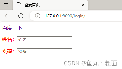
之前写过VGA,其实HDMI也写过,但是没记笔记。
VGA时序
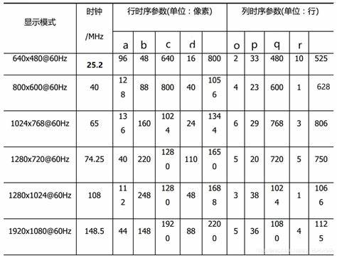
VGA Signal Timing (tinyvga.com)
介绍 
规范:
小结:
VGA像素编码以后通过差分对端口以十倍像素时钟的速率地串行发送。
官方例程
HDMI编码器
来自xaap460的编码器
//
//
//  Xilinx, Inc. 2008                 www.xilinx.com
//
//
//
//  File name :       encode.v
//
//  Description :     TMDS encoder
//
//  Date - revision : Jan. 2008 - v 1.0
//
//  Author :          Bob Feng
//
//  Disclaimer: LIMITED WARRANTY AND DISCLAMER. These designs are
//              provided to you "as is". Xilinx and its licensors make and you
//              receive no warranties or conditions, express, implied,
//              statutory or otherwise, and Xilinx specifically disclaims any
//              implied warranties of merchantability, non-infringement,or
//              fitness for a particular purpose. Xilinx does not warrant that
//              the functions contained in these designs will meet your
//              requirements, or that the operation of these designs will be
//              uninterrupted or error free, or that defects in the Designs
//              will be corrected. Furthermore, Xilinx does not warrantor
//              make any representations regarding use or the results of the
//              use of the designs in terms of correctness, accuracy,
//              reliability, or otherwise.
//
//              LIMITATION OF LIABILITY. In no event will Xilinx or its
//              licensors be liable for any loss of data, lost profits,cost
//              or procurement of substitute goods or services, or for any
//              special, incidental, consequential, or indirect damages
//              arising from the use or operation of the designs or
//              accompanying documentation, however caused and on any theory
//              of liability. This limitation will apply even if Xilinx
//              has been advised of the possibility of such damage. This
//              limitation shall apply not-withstanding the failure of the
//              essential purpose of any limited remedies herein.
//
//  Copyright � 2006 Xilinx, Inc.
//  All rights reserved
//
//
`timescale 1 ps / 1ps

module encode (
  input            clkin,    // pixel clock input
  input            rstin,    // async. reset input (active high)
  input      [7:0] din,      // data inputs: expect registered
  input            c0,       // c0 input
  input            c1,       // c1 input
  input            de,       // de input
  output reg [9:0] dout      // data outputs
);


  // Counting number of 1s and 0s for each incoming pixel
  // component. Pipe line the result.
  // Register Data Input so it matches the pipe lined adder
  // output

  reg [3:0] n1d; //number of 1s in din
  reg [7:0] din_q;

  always @ (posedge clkin) begin
    n1d <=#1 din[0] + din[1] + din[2] + din[3] + din[4] + din[5] + din[6] + din[7];

    din_q <=#1 din;
  end

  ///
  // Stage 1: 8 bit -> 9 bit
  // Refer to DVI 1.0 Specification, page 29, Figure 3-5
  ///
  wire decision1;

  assign decision1 = (n1d > 4'h4) | ((n1d == 4'h4) & (din_q[0] == 1'b0));
/*
  reg [8:0] q_m;
  always @ (posedge clkin) begin
    q_m[0] <=#1 din_q[0];
    q_m[1] <=#1 (decision1) ? (q_m[0] ^~ din_q[1]) : (q_m[0] ^ din_q[1]);
    q_m[2] <=#1 (decision1) ? (q_m[1] ^~ din_q[2]) : (q_m[1] ^ din_q[2]);
    q_m[3] <=#1 (decision1) ? (q_m[2] ^~ din_q[3]) : (q_m[2] ^ din_q[3]);
    q_m[4] <=#1 (decision1) ? (q_m[3] ^~ din_q[4]) : (q_m[3] ^ din_q[4]);
    q_m[5] <=#1 (decision1) ? (q_m[4] ^~ din_q[5]) : (q_m[4] ^ din_q[5]);
    q_m[6] <=#1 (decision1) ? (q_m[5] ^~ din_q[6]) : (q_m[5] ^ din_q[6]);
    q_m[7] <=#1 (decision1) ? (q_m[6] ^~ din_q[7]) : (q_m[6] ^ din_q[7]);
    q_m[8] <=#1 (decision1) ? 1'b0 : 1'b1;
  end
*/
  wire [8:0] q_m;
  assign q_m[0] = din_q[0];
  assign q_m[1] = (decision1) ? (q_m[0] ^~ din_q[1]) : (q_m[0] ^ din_q[1]);
  assign q_m[2] = (decision1) ? (q_m[1] ^~ din_q[2]) : (q_m[1] ^ din_q[2]);
  assign q_m[3] = (decision1) ? (q_m[2] ^~ din_q[3]) : (q_m[2] ^ din_q[3]);
  assign q_m[4] = (decision1) ? (q_m[3] ^~ din_q[4]) : (q_m[3] ^ din_q[4]);
  assign q_m[5] = (decision1) ? (q_m[4] ^~ din_q[5]) : (q_m[4] ^ din_q[5]);
  assign q_m[6] = (decision1) ? (q_m[5] ^~ din_q[6]) : (q_m[5] ^ din_q[6]);
  assign q_m[7] = (decision1) ? (q_m[6] ^~ din_q[7]) : (q_m[6] ^ din_q[7]);
  assign q_m[8] = (decision1) ? 1'b0 : 1'b1;

  /
  // Stage 2: 9 bit -> 10 bit
  // Refer to DVI 1.0 Specification, page 29, Figure 3-5
  /
  reg [3:0] n1q_m, n0q_m; // number of 1s and 0s for q_m
  always @ (posedge clkin) begin
    n1q_m  <=#1 q_m[0] + q_m[1] + q_m[2] + q_m[3] + q_m[4] + q_m[5] + q_m[6] + q_m[7];
    n0q_m  <=#1 4'h8 - (q_m[0] + q_m[1] + q_m[2] + q_m[3] + q_m[4] + q_m[5] + q_m[6] + q_m[7]);
  end

  parameter CTRLTOKEN0 = 10'b1101010100;
  parameter CTRLTOKEN1 = 10'b0010101011;
  parameter CTRLTOKEN2 = 10'b0101010100;
  parameter CTRLTOKEN3 = 10'b1010101011;

  reg [4:0] cnt; //disparity counter, MSB is the sign bit
  wire decision2, decision3;

  assign decision2 = (cnt == 5'h0) | (n1q_m == n0q_m);
  /
  // [(cnt > 0) and (N1q_m > N0q_m)] or [(cnt < 0) and (N0q_m > N1q_m)]
  /
  assign decision3 = (~cnt[4] & (n1q_m > n0q_m)) | (cnt[4] & (n0q_m > n1q_m));


  // pipe line alignment

  reg       de_q, de_reg;
  reg       c0_q, c1_q;
  reg       c0_reg, c1_reg;
  reg [8:0] q_m_reg;

  always @ (posedge clkin) begin
    de_q    <=#1 de;
    de_reg  <=#1 de_q;

    c0_q    <=#1 c0;
    c0_reg  <=#1 c0_q;
    c1_q    <=#1 c1;
    c1_reg  <=#1 c1_q;

    q_m_reg <=#1 q_m;
  end

  ///
  // 10-bit out
  // disparity counter
  ///
  always @ (posedge clkin or posedge rstin) begin
    if(rstin) begin
      dout <= 10'h0;
      cnt <= 5'h0;
    end else begin
      if (de_reg) begin
        if(decision2) begin
          dout[9]   <=#1 ~q_m_reg[8];
          dout[8]   <=#1 q_m_reg[8];
          dout[7:0] <=#1 (q_m_reg[8]) ? q_m_reg[7:0] : ~q_m_reg[7:0];

          cnt <=#1 (~q_m_reg[8]) ? (cnt + n0q_m - n1q_m) : (cnt + n1q_m - n0q_m);
        end else begin
          if(decision3) begin
            dout[9]   <=#1 1'b1;
            dout[8]   <=#1 q_m_reg[8];
            dout[7:0] <=#1 ~q_m_reg;

            cnt <=#1 cnt + {q_m_reg[8], 1'b0} + (n0q_m - n1q_m);
          end else begin
            dout[9]   <=#1 1'b0;
            dout[8]   <=#1 q_m_reg[8];
            dout[7:0] <=#1 q_m_reg[7:0];

            cnt <=#1 cnt - {~q_m_reg[8], 1'b0} + (n1q_m - n0q_m);
          end
        end
      end else begin
        case ({c1_reg, c0_reg})
          2'b00:   dout <=#1 CTRLTOKEN0;
          2'b01:   dout <=#1 CTRLTOKEN1;
          2'b10:   dout <=#1 CTRLTOKEN2;
          default: dout <=#1 CTRLTOKEN3;
        endcase

        cnt <=#1 5'h0;
      end
    end
  end

endmodule
串转并
//
//
//  Xilinx, Inc. 2007                 www.xilinx.com
//
//
//
//  File name :       serdes_4b_10to1.v
//
//  Description :     4-bit transmitter macro for Spartan 3A (uses ODDR2)
//      Takes in 30 bits and serialises this to 4 bits DDR (4th bit is a regenerated clock)
//
//      data is transmitted LSBs first
//      0, 3,  6,  9, 12, 15, 18, 21, 24, 27 - data
//      1, 4,  7, 10, 13, 16, 19, 22, 25, 28 - data
//      2, 5,  8, 11, 14, 17, 20, 23, 26, 29 - data
//      0, 0,  0,  0,  0,  1,  1,  1,  1,  1 - clock
//
//
//  Author :          Bob Feng
//  Disclaimer: LIMITED WARRANTY AND DISCLAMER. These designs are
//              provided to you "as is". Xilinx and its licensors make, and you
//              receive no warranties or conditions, express, implied,
//              statutory or otherwise, and Xilinx specifically disclaims any
//              implied warranties of merchantability, non-infringement, or
//              fitness for a particular purpose. Xilinx does not warrant that
//              the functions contained in these designs will meet your
//              requirements, or that the operation of these designs will be
//              uninterrupted or error free, or that defects in the Designs
//              will be corrected. Furthermore, Xilinx does not warrant or
//              make any representations regarding use or the results of the
//              use of the designs in terms of correctness, accuracy,
//              reliability, or otherwise.
//
//              LIMITATION OF LIABILITY. In no event will Xilinx or its
//              licensors be liable for any loss of data, lost profits, cost
//              or procurement of substitute goods or services, or for any
//              special, incidental, consequential, or indirect damages
//              arising from the use or operation of the designs or
//              accompanying documentation, however caused and on any theory
//              of liability. This limitation will apply even if Xilinx
//              has been advised of the possibility of such damage. This
//              limitation shall apply not-withstanding the failure of the
//              essential purpose of any limited remedies herein.
//
//  Copyright � 2007 Xilinx, Inc.
//  All rights reserved
//
//
`timescale 1ns/1ps

module serdes_4b_10to1 (
  input          clk,         // clock input
  input          clkx5,       // 5x clock input
  input          clkx5not,
  input [29:0]   datain,      // input data for serialisation
  input          rst,         // reset
  output [7:0]   dataout) ;   // out DDR data and clock

  wire [4:0] syncp; // internal sync signals for rising edges
  wire [4:0] syncn; // internal sync signals for falling edges

  reg [3:0] p_mux;      // muxes (+ve)
  reg [3:0] n_mux;      // muxes (-ve)
  wire [29:0] dataint;
  wire [29:0] db;

  wire  [3:0]   wa;       // RAM read address
  reg   [3:0]   wa_d;     // RAM read address
  wire  [3:0]   ra;       // RAM read address
  reg   [3:0]   ra_d;     // RAM read address


  // Here we instantiate a 16x30 Dual Port RAM
  // and fill first it with data aligned to
  // clk domain


  parameter ADDR0  = 4'b0000;
  parameter ADDR1  = 4'b0001;
  parameter ADDR2  = 4'b0010;
  parameter ADDR3  = 4'b0011;
  parameter ADDR4  = 4'b0100;
  parameter ADDR5  = 4'b0101;
  parameter ADDR6  = 4'b0110;
  parameter ADDR7  = 4'b0111;
  parameter ADDR8  = 4'b1000;
  parameter ADDR9  = 4'b1001;
  parameter ADDR10 = 4'b1010;
  parameter ADDR11 = 4'b1011;
  parameter ADDR12 = 4'b1100;
  parameter ADDR13 = 4'b1101;
  parameter ADDR14 = 4'b1110;
  parameter ADDR15 = 4'b1111;

  always@(wa) begin
    case (wa)
      ADDR0   : wa_d = ADDR1 ;
      ADDR1   : wa_d = ADDR2 ;
      ADDR2   : wa_d = ADDR3 ;
      ADDR3   : wa_d = ADDR4 ;
      ADDR4   : wa_d = ADDR5 ;
      ADDR5   : wa_d = ADDR6 ;
      ADDR6   : wa_d = ADDR7 ;
      ADDR7   : wa_d = ADDR8 ;
      ADDR8   : wa_d = ADDR9 ;
      ADDR9   : wa_d = ADDR10;
      ADDR10  : wa_d = ADDR11;
      ADDR11  : wa_d = ADDR12;
      ADDR12  : wa_d = ADDR13;
      ADDR13  : wa_d = ADDR14;
      ADDR14  : wa_d = ADDR15;
      default : wa_d = ADDR0;
    endcase
  end

  FDC fdc_wa0 (.C(clk),  .D(wa_d[0]), .CLR(rst), .Q(wa[0]));
  FDC fdc_wa1 (.C(clk),  .D(wa_d[1]), .CLR(rst), .Q(wa[1]));
  FDC fdc_wa2 (.C(clk),  .D(wa_d[2]), .CLR(rst), .Q(wa[2]));
  FDC fdc_wa3 (.C(clk),  .D(wa_d[3]), .CLR(rst), .Q(wa[3]));

  //Dual Port fifo to bridge data through
  DRAM16XN #(.data_width(30))
  fifo_u (
         .DATA_IN(datain),
         .ADDRESS(wa),
         .ADDRESS_DP(ra),
         .WRITE_EN(1'b1),
         .CLK(clk),
         .O_DATA_OUT(),
         .O_DATA_OUT_DP(dataint));

  /
  // Here starts clk5x domain for fifo read out
  // FIFO read is set to be once every 5 cycles of clk5x in order
  // to keep up pace with the fifo write speed
  // Also FIFO read reset is delayed a bit in order to avoid
  // underflow.
  /

  always@(ra) begin
    case (ra)
      ADDR0   : ra_d = ADDR1 ;
      ADDR1   : ra_d = ADDR2 ;
      ADDR2   : ra_d = ADDR3 ;
      ADDR3   : ra_d = ADDR4 ;
      ADDR4   : ra_d = ADDR5 ;
      ADDR5   : ra_d = ADDR6 ;
      ADDR6   : ra_d = ADDR7 ;
      ADDR7   : ra_d = ADDR8 ;
      ADDR8   : ra_d = ADDR9 ;
      ADDR9   : ra_d = ADDR10;
      ADDR10  : ra_d = ADDR11;
      ADDR11  : ra_d = ADDR12;
      ADDR12  : ra_d = ADDR13;
      ADDR13  : ra_d = ADDR14;
      ADDR14  : ra_d = ADDR15;
      default : ra_d = ADDR0;
    endcase
  end

  wire rstsync, rstsync_q, rstp, rstn;
  (* ASYNC_REG = "TRUE" *) FDP fdp_rst  (.C(clkx5),  .D(rst), .PRE(rst), .Q(rstsync));

  FD fd_rstsync (.C(clkx5),  .D(rstsync), .Q(rstsync_q));
  FD fd_rstp    (.C(clkx5),  .D(rstsync_q), .Q(rstp));

  FDRE fdc_ra0 (.C(clkx5),  .D(ra_d[0]), .R(rstp), .CE(syncp[4]), .Q(ra[0]));
  FDRE fdc_ra1 (.C(clkx5),  .D(ra_d[1]), .R(rstp), .CE(syncp[4]), .Q(ra[1]));
  FDRE fdc_ra2 (.C(clkx5),  .D(ra_d[2]), .R(rstp), .CE(syncp[4]), .Q(ra[2]));
  FDRE fdc_ra3 (.C(clkx5),  .D(ra_d[3]), .R(rstp), .CE(syncp[4]), .Q(ra[3]));

  //
  // 5 Cycle Counter for clkx5
  // Generate data latch and bit mux timing
  //
  wire [2:0] statep, staten;
  reg [2:0] statep_d, staten_d;

  parameter ST0 = 3'b000;
  parameter ST1 = 3'b001;
  parameter ST2 = 3'b011;
  parameter ST3 = 3'b111;
  parameter ST4 = 3'b110;

  always@(statep) begin
    case (statep)
      ST0     : statep_d = ST1 ;
      ST1     : statep_d = ST2 ;
      ST2     : statep_d = ST3 ;
      ST3     : statep_d = ST4 ;
      default : statep_d = ST0;
    endcase
  end

  FDR fdc_stp0 (.C(clkx5),  .D(statep_d[0]), .R(rstp), .Q(statep[0]));
  FDR fdc_stp1 (.C(clkx5),  .D(statep_d[1]), .R(rstp), .Q(statep[1]));
  FDR fdc_stp2 (.C(clkx5),  .D(statep_d[2]), .R(rstp), .Q(statep[2]));

  wire [4:0] syncp_d;

  assign syncp_d[0] = (statep == ST0);
  assign syncp_d[1] = (statep == ST1);
  assign syncp_d[2] = (statep == ST2);
  assign syncp_d[3] = (statep == ST3);
  assign syncp_d[4] = (statep == ST4);

  FD fd_syncp0 (.C(clkx5), .D(syncp_d[0]), .Q(syncp[0]));
  FD fd_syncp1 (.C(clkx5), .D(syncp_d[1]), .Q(syncp[1]));
  FD fd_syncp2 (.C(clkx5), .D(syncp_d[2]), .Q(syncp[2]));
  FD fd_syncp3 (.C(clkx5), .D(syncp_d[3]), .Q(syncp[3]));
  FD fd_syncp4 (.C(clkx5), .D(syncp_d[4]), .Q(syncp[4]));

  //
  // 5 Cycle Counter for clkx5not
  // Generate data latch and bit mux timing
  //
  FD  fd_rstn (.C(clkx5not),  .D(rstsync_q), .Q(rstn));

  always@(staten) begin
    case (staten)
      ST0     : staten_d = ST1 ;
      ST1     : staten_d = ST2 ;
      ST2     : staten_d = ST3 ;
      ST3     : staten_d = ST4 ;
      default : staten_d = ST0;
    endcase
  end

  FDR fdc_stn0 (.C(clkx5not),  .D(staten_d[0]), .R(rstn), .Q(staten[0]));
  FDR fdc_stn1 (.C(clkx5not),  .D(staten_d[1]), .R(rstn), .Q(staten[1]));
  FDR fdc_stn2 (.C(clkx5not),  .D(staten_d[2]), .R(rstn), .Q(staten[2]));

  wire [4:0] syncn_d;

  assign syncn_d[0] = (staten == ST0);
  assign syncn_d[1] = (staten == ST1);
  assign syncn_d[2] = (staten == ST2);
  assign syncn_d[3] = (staten == ST3);
  assign syncn_d[4] = (staten == ST4);

  FD fd_syncn0 (.C(clkx5not), .D(syncn_d[0]), .Q(syncn[0]));
  FD fd_syncn1 (.C(clkx5not), .D(syncn_d[1]), .Q(syncn[1]));
  FD fd_syncn2 (.C(clkx5not), .D(syncn_d[2]), .Q(syncn[2]));
  FD fd_syncn3 (.C(clkx5not), .D(syncn_d[3]), .Q(syncn[3]));
  FD fd_syncn4 (.C(clkx5not), .D(syncn_d[4]), .Q(syncn[4]));


  // Latch data out of FIFO
  // clkx5 setup time: 5 cycles since syncp[4] is used as CE
  // clkx5not setup time: 4.5 cycles since syncn[4] is used as CE
  // syncn[4] is set to be 0.5 cycle earlier than syncp[4]

  FDE fd_db0 (.C(clkx5not), .D(dataint[0]),  .CE(syncn[4]), .Q(db[0]));
  FDE fd_db1 (.C(clkx5not), .D(dataint[1]),  .CE(syncn[4]), .Q(db[1]));
  FDE fd_db2 (.C(clkx5not), .D(dataint[2]),  .CE(syncn[4]), .Q(db[2]));

  FDE fd_db3 (.C(clkx5),    .D(dataint[3]),  .CE(syncp[4]), .Q(db[3]));
  FDE fd_db4 (.C(clkx5),    .D(dataint[4]),  .CE(syncp[4]), .Q(db[4]));
  FDE fd_db5 (.C(clkx5),    .D(dataint[5]),  .CE(syncp[4]), .Q(db[5]));

  FDE fd_db6 (.C(clkx5not), .D(dataint[6]),  .CE(syncn[4]), .Q(db[6]));
  FDE fd_db7 (.C(clkx5not), .D(dataint[7]),  .CE(syncn[4]), .Q(db[7]));
  FDE fd_db8 (.C(clkx5not), .D(dataint[8]),  .CE(syncn[4]), .Q(db[8]));

  FDE fd_db9 (.C(clkx5),    .D(dataint[9]),  .CE(syncp[4]), .Q(db[9]));
  FDE fd_db10(.C(clkx5),    .D(dataint[10]), .CE(syncp[4]), .Q(db[10]));
  FDE fd_db11(.C(clkx5),    .D(dataint[11]), .CE(syncp[4]), .Q(db[11]));

  FDE fd_db12(.C(clkx5not), .D(dataint[12]), .CE(syncn[4]), .Q(db[12]));
  FDE fd_db13(.C(clkx5not), .D(dataint[13]), .CE(syncn[4]), .Q(db[13]));
  FDE fd_db14(.C(clkx5not), .D(dataint[14]), .CE(syncn[4]), .Q(db[14]));

  FDE fd_db15(.C(clkx5),    .D(dataint[15]), .CE(syncp[4]), .Q(db[15]));
  FDE fd_db16(.C(clkx5),    .D(dataint[16]), .CE(syncp[4]), .Q(db[16]));
  FDE fd_db17(.C(clkx5),    .D(dataint[17]), .CE(syncp[4]), .Q(db[17]));

  FDE fd_db18(.C(clkx5not), .D(dataint[18]), .CE(syncn[4]), .Q(db[18]));
  FDE fd_db19(.C(clkx5not), .D(dataint[19]), .CE(syncn[4]), .Q(db[19]));
  FDE fd_db20(.C(clkx5not), .D(dataint[20]), .CE(syncn[4]), .Q(db[20]));

  FDE fd_db21(.C(clkx5),    .D(dataint[21]), .CE(syncp[4]), .Q(db[21]));
  FDE fd_db22(.C(clkx5),    .D(dataint[22]), .CE(syncp[4]), .Q(db[22]));
  FDE fd_db23(.C(clkx5),    .D(dataint[23]), .CE(syncp[4]), .Q(db[23]));

  FDE fd_db24(.C(clkx5not), .D(dataint[24]), .CE(syncn[4]), .Q(db[24]));
  FDE fd_db25(.C(clkx5not), .D(dataint[25]), .CE(syncn[4]), .Q(db[25]));
  FDE fd_db26(.C(clkx5not), .D(dataint[26]), .CE(syncn[4]), .Q(db[26]));

  FDE fd_db27(.C(clkx5),    .D(dataint[27]), .CE(syncp[4]), .Q(db[27]));
  FDE fd_db28(.C(clkx5),    .D(dataint[28]), .CE(syncp[4]), .Q(db[28]));
  FDE fd_db29(.C(clkx5),    .D(dataint[29]), .CE(syncp[4]), .Q(db[29]));

  //
  // Data OUT Multiplexers: clk5x and clk5xnot
  //
  always @ (*)
  begin
    casex (1'b1) // synthesis parallel_case full_case
      syncn[0]: begin
        n_mux[0] = db[0];
        n_mux[1] = db[1];
        n_mux[2] = db[2];
        n_mux[3] = 1'b0;
      end

      syncn[1]: begin
        n_mux[0] = db[6];
        n_mux[1] = db[7];
        n_mux[2] = db[8];
        n_mux[3] = 1'b0;
      end

      syncn[2]: begin
        n_mux[0] = db[12];
        n_mux[1] = db[13];
        n_mux[2] = db[14];
        n_mux[3] = 1'b0;
      end

      syncn[3]: begin
        n_mux[0] = db[18];
        n_mux[1] = db[19];
        n_mux[2] = db[20];
        n_mux[3] = 1'b1;
      end

      syncn[4]: begin
        n_mux[0] = db[24];
        n_mux[1] = db[25];
        n_mux[2] = db[26];
        n_mux[3] = 1'b1;
      end
    endcase
  end

  FD muxn0(.D(n_mux[0]), .C(clkx5not), .Q(dataout[4])) ;
  FD muxn1(.D(n_mux[1]), .C(clkx5not), .Q(dataout[5])) ;
  FD muxn2(.D(n_mux[2]), .C(clkx5not), .Q(dataout[6])) ;
  FD muxn3(.D(n_mux[3]), .C(clkx5not), .Q(dataout[7])) ;

  always @ (*)
  begin
    casex (1'b1) // synthesis parallel_case full_case
      syncp[0]: begin
        p_mux[0] = db[3];
        p_mux[1] = db[4];
        p_mux[2] = db[5];
        p_mux[3] = 1'b0;
      end

      syncp[1]: begin
        p_mux[0] = db[9];
        p_mux[1] = db[10];
        p_mux[2] = db[11];
        p_mux[3] = 1'b0;
      end

      syncp[2]: begin
        p_mux[0] = db[15];
        p_mux[1] = db[16];
        p_mux[2] = db[17];
        p_mux[3] = 1'b1;
      end

      syncp[3]: begin
        p_mux[0] = db[21];
        p_mux[1] = db[22];
        p_mux[2] = db[23];
        p_mux[3] = 1'b1;
      end

      syncp[4]: begin
        p_mux[0] = db[27];
        p_mux[1] = db[28];
        p_mux[2] = db[29];
        p_mux[3] = 1'b1;
      end
    endcase
  end

  FD muxp0(.D(p_mux[0]), .C(clkx5), .Q(dataout[0])) ;
  FD muxp1(.D(p_mux[1]), .C(clkx5), .Q(dataout[1])) ;
  FD muxp2(.D(p_mux[2]), .C(clkx5), .Q(dataout[2])) ;
  FD muxp3(.D(p_mux[3]), .C(clkx5), .Q(dataout[3])) ;

endmodule
原语OSERDESE2
两个OSERDESE2的串联方法
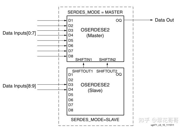
OSERDESE2_Master (
    .CLK        (serial_clk_5x),    // 串行数据时钟,5倍时钟频率
    .CLKDIV     (paralell_clk),     // 并行数据时钟
    .RST        (reset),            // 1-bit input: Reset
    .OCE        (1'b1),             // 1-bit input: Output data clock enable

    .OQ         (serial_data_out),  // 串行输出数据

    .D1         (paralell_data[0]), // D1 - D8: 并行数据输入
    .D2         (paralell_data[1]),
    .D3         (paralell_data[2]),
    .D4         (paralell_data[3]),
    .D5         (paralell_data[4]),
    .D6         (paralell_data[5]),
    .D7         (paralell_data[6]),
    .D8         (paralell_data[7]),

    .SHIFTIN1   (cascade1),         // SHIFTIN1 用于位宽扩展
    .SHIFTIN2   (cascade2),         // SHIFTIN2
    .SHIFTOUT1  (),                 // SHIFTOUT1: 用于位宽扩展
    .SHIFTOUT2  (),                 // SHIFTOUT2

    .OFB        (),                 // 以下是未使用信号
    .T1         (1'b0),
    .T2         (1'b0),
    .T3         (1'b0),
    .T4         (1'b0),
    .TBYTEIN    (1'b0),
    .TCE        (1'b0),
    .TBYTEOUT   (),
    .TFB        (),
    .TQ         ()
);

//例化OSERDESE2原语,实现并串转换,Slave模式
OSERDESE2 #(
    .DATA_RATE_OQ   ("DDR"),       // 设置双倍数据速率
    .DATA_RATE_TQ   ("SDR"),       // DDR, BUF, SDR
    .DATA_WIDTH     (10),           // 输入的并行数据宽度为10bit
    .SERDES_MODE    ("SLAVE"),     // 设置为Slave,用于10bit宽度扩展
    .TBYTE_CTL      ("FALSE"),     // Enable tristate byte operation (FALSE, TRUE)
    .TBYTE_SRC      ("FALSE"),     // Tristate byte source (FALSE, TRUE)
    .TRISTATE_WIDTH (1)             // 3-state converter width (1,4)
)
OSERDESE2_Slave (
    .CLK        (serial_clk_5x),    // 串行数据时钟,5倍时钟频率
    .CLKDIV     (paralell_clk),     // 并行数据时钟
    .RST        (reset),            // 1-bit input: Reset
    .OCE        (1'b1),             // 1-bit input: Output data clock enable

    .OQ         (),                 // 串行输出数据

    .D1         (1'b0),             // D1 - D8: 并行数据输入
    .D2         (1'b0),
    .D3         (paralell_data[8]),
    .D4         (paralell_data[9]),
    .D5         (1'b0),
    .D6         (1'b0),
    .D7         (1'b0),
    .D8         (1'b0),

    .SHIFTIN1   (),                 // SHIFTIN1 用于位宽扩展
    .SHIFTIN2   (),                 // SHIFTIN2
    .SHIFTOUT1  (cascade1),         // SHIFTOUT1: 用于位宽扩展
    .SHIFTOUT2  (cascade2),         // SHIFTOUT2

    .OFB        (),                 // 以下是未使用信号
    .T1         (1'b0),
    .T2         (1'b0),
    .T3         (1'b0),
    .T4         (1'b0),
    .TBYTEIN    (1'b0),
    .TCE        (1'b0),
    .TBYTEOUT   (),
    .TFB        (),
    .TQ         ()
);
原语OBUFDS
用例
//
//
//  Xilinx, Inc. 2007                 www.xilinx.com
//
//  XAPP xyz
//
//
//
//  File name :       dvi_encoder.v
//
//  Description :     dvi_encoder
//
//  Date - revision : Feb. 2008 - 1.0.0
//
//  Author :          Bob Feng
//
//  Disclaimer: LIMITED WARRANTY AND DISCLAMER. These designs are
//              provided to you "as is". Xilinx and its licensors makeand you
//              receive no warranties or conditions, express, implied,
//              statutory or otherwise, and Xilinx specificallydisclaims any
//              implied warranties of merchantability, non-infringement,or
//              fitness for a particular purpose. Xilinx does notwarrant that
//              the functions contained in these designs will meet your
//              requirements, or that the operation of these designswill be
//              uninterrupted or error free, or that defects in theDesigns
//              will be corrected. Furthermore, Xilinx does not warrantor
//              make any representations regarding use or the results ofthe
//              use of the designs in terms of correctness, accuracy,
//              reliability, or otherwise.
//
//              LIMITATION OF LIABILITY. In no event will Xilinx or its
//              licensors be liable for any loss of data, lost profits,cost
//              or procurement of substitute goods or services, or forany
//              special, incidental, consequential, or indirect damages
//              arising from the use or operation of the designs or
//              accompanying documentation, however caused and on anytheory
//              of liability. This limitation will apply even if Xilinx
//              has been advised of the possibility of such damage. This
//              limitation shall apply not-withstanding the failure ofthe
//              essential purpose of any limited remedies herein.
//
//  Copyright � 2004 Xilinx, Inc.
//  All rights reserved
//
//
`timescale 1 ps / 1ps

module dvi_encoder # (
  parameter SDATAINVERT = "FALSE" //Invert or not SDATA before serilize it
)(
input				clkin,			// system clock
input				clkx5in,		// system clock x5
input     			clkx5notin, 	// system clock x5 not
input				rstin,			// reset
input		[7:0]	blue_din,		// Blue data in
input		[7:0]	green_din,		// Green data in
input		[7:0]	red_din,		// Red data in
input				hsync,			// hsync data
input				vsync,			// vsync data
input				de,				// data enable
output		[7:0]	tmds_data) ;	// data outputs to ddr in IOB, bit 3(and 7) is clock

wire 	[9:0]	red ;
wire 	[9:0]	green ;
wire 	[9:0]	blue ;
wire 	[29:0]	s_data ;

encode encb (
	.clkin		(clkin),
	.rstin		(rstin),
	.din		(blue_din),
	.c0			(hsync),
	.c1			(vsync),
	.de			(de),
	.dout		(blue)) ;

encode encr (
	.clkin	(clkin),
	.rstin	(rstin),
	.din	(green_din),
	.c0		(1'b0),
	.c1		(1'b0),
	.de		(de),
	.dout	(green)) ;

encode encg (
	.clkin	(clkin),
	.rstin	(rstin),
	.din		(red_din),
	.c0			(1'b0),
	.c1			(1'b0),
	.de			(de),
	.dout		(red)) ;

assign s_data = {red[9], green[9], blue[9], red[8], green[8], blue[8],
	   	 red[7], green[7], blue[7], red[6], green[6], blue[6],
	   	 red[5], green[5], blue[5], red[4], green[4], blue[4],
	   	 red[3], green[3], blue[3], red[2], green[2], blue[2],
	   	 red[1], green[1], blue[1], red[0], green[0], blue[0]} ;

reg [29:0] s_data_q;

always @ (posedge clkin) begin
  if(SDATAINVERT == "TRUE")
    s_data_q <= ~s_data;
  else
    s_data_q <= s_data;
end

serdes_4b_10to1 serialise (
	.clk		(clkin),
	.clkx5		(clkx5in),
	.clkx5not	(clkx5notin),
	.datain		(s_data_q),
	.rst		(rstin),
	.dataout	(tmds_data)) ;

endmodule