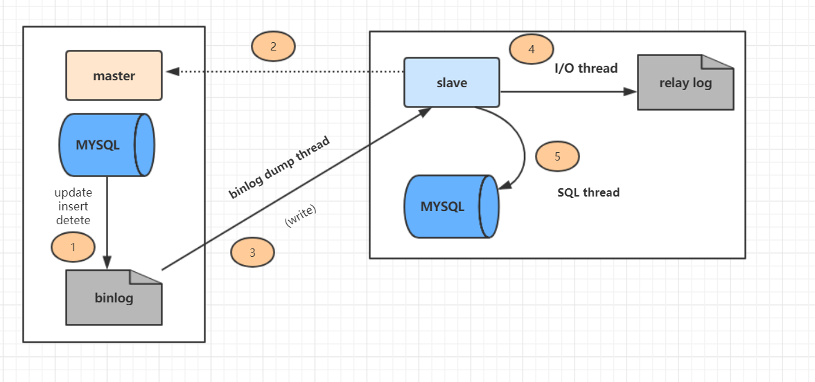
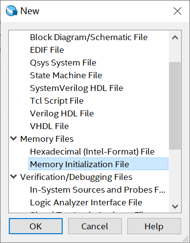
quartus工具篇——ROM ip核
1、ROM简介
FPGA中的ROM(Read-Only Memory)是一种只读存储器,主要用来存储固化的初始化配置数据。FPGA ROM的特性主要有:
- 预编程初始化 - ROM在FPGA编程时就已经写入了初始值,这些值在整个工作周期保持不变。
- 初始化配置 - ROM通常用来存储FPGA的初始配置文件或者开机激励向量。
- 单端口访问 - ROM通常只提供数据输出接口,不可写入。
- 高密度 - 利用定制流程可以实现非常高密度的ROM。
- 封闭保密 - ROM存储的数据无法被读取,保证了配置或代码的保密性。
- 提高可靠性 - ROM存储更加稳定可靠,不会像RAM丢失数据。
- 加速启动 - ROM存储的初始化文件可以加速FPGA的启动配置。
- 降低成本 - ROM的制造成本低于RAM。
在许多需求可靠启动和保密的应用中,FPGA通过内置ROM提供了有效的特性实现。它主要作为一种只读非易失的初始化存储器使用。
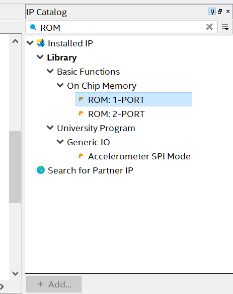
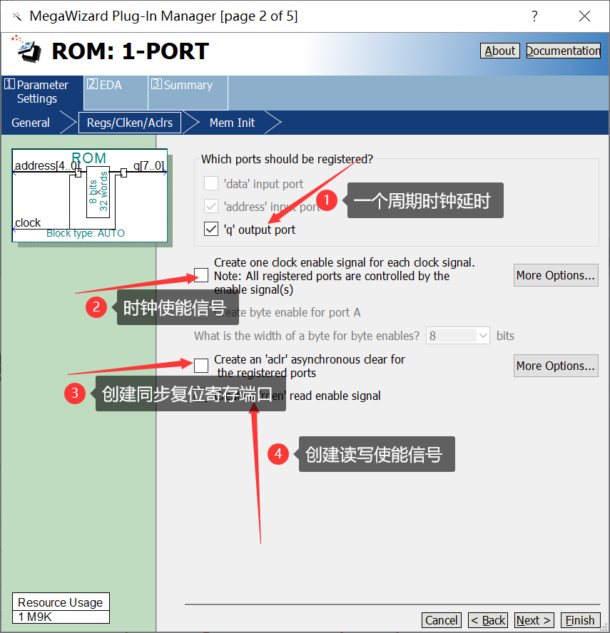
2、ROM IP核的配置
在quartus右上栏搜索ROM,双击打开并命令,如下图:
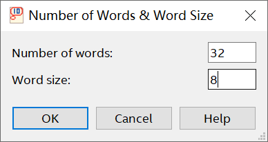
设置内存单元大小和需要的内存单元
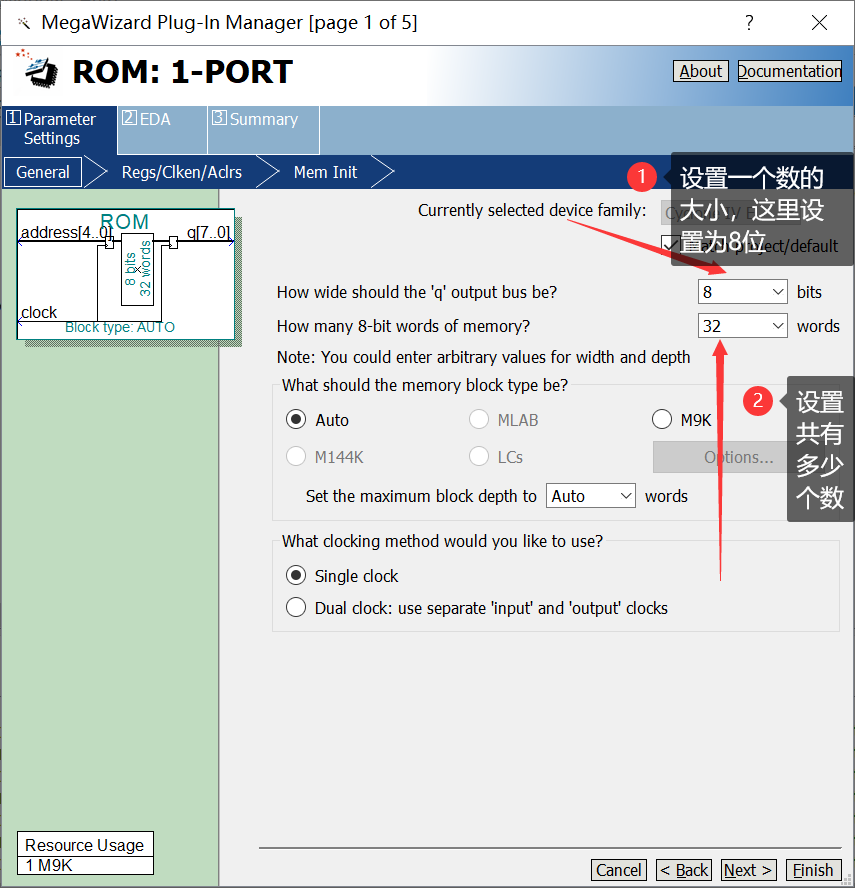
按照下图进行配置
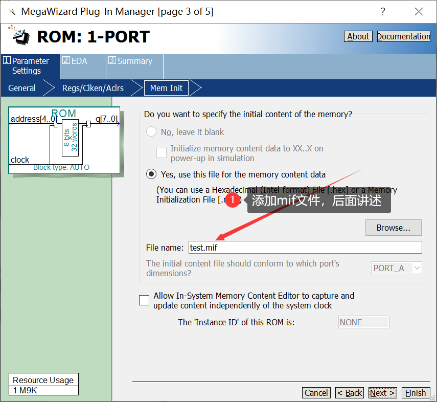
添加mif文件
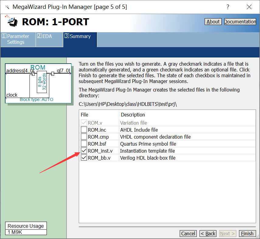
勾上选项,进行生成模块实例文件
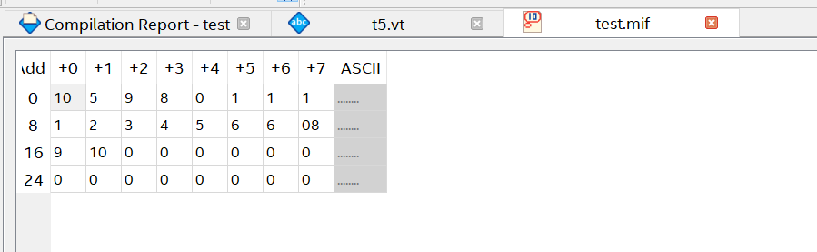
3、mif文件生成
部分简单的Mif文件我们 可以自己插入数据,比较复杂的就需要应用程序进行生成
简单的数据:
在quartus中生成mif文件
和我们在ip核配置的内存大小和内存个数要相同
自行编辑文件,如下图我编辑的结果
c语言生成Mif文件,我这里gpt生成的效果可能不好,可以自行去网上找一个
#include <stdio.h>

int main() {

  FILE *fptr;
  fptr = fopen("ram_init.mif","w");

  fprintf(fptr,"WIDTH=16;\n");
  fprintf(fptr,"DEPTH=128;\n\n");

  int i;
  for(i=0; i<128; i++) {
    fprintf(fptr,"%02X : %04X;\n", i, i*2);
  }

  fclose(fptr);

  return 0;
}
mif文件弄好后重新编辑ip核即可
3、仿真代码编写
// Copyright (C) 2018  Intel Corporation. All rights reserved.
// Your use of Intel Corporation's design tools, logic functions
// and other software and tools, and its AMPP partner logic
// functions, and any output files from any of the foregoing
// (including device programming or simulation files), and any
// associated documentation or information are expressly subject
// to the terms and conditions of the Intel Program License
// Subscription Agreement, the Intel Quartus Prime License Agreement,
// the Intel FPGA IP License Agreement, or other applicable license
// agreement, including, without limitation, that your use is for
// the sole purpose of programming logic devices manufactured by
// Intel and sold by Intel or its authorized distributors.  Please
// refer to the applicable agreement for further details.

// *****************************************************************************
// This file contains a Verilog test bench template that is freely editable to
// suit user's needs .Comments are provided in each section to help the user
// fill out necessary details.
// *****************************************************************************
// Generated on "07/24/2023 19:18:12"

// Verilog Test Bench template for design : t5
//
// Simulation tool : ModelSim-Altera (Verilog)
//

`timescale 1 ns/ 1 ns
module t5_vlg_tst();

parameter SYS_CLK = 20;
reg clk;
wire[7:0] read_data;
reg[4:0] address = 1'b0;

always #(SYS_CLK/2) clk = ~clk;
integer i;
initial begin
    clk = 1'b0;
    for(i = 0;i<31;i=i+1)begin
        #(SYS_CLK*2)
        address = address+1'b1;
    end
    #(20*SYS_CLK);
    $stop;
end

ROM ROM_inst (
    .address ( address ),
    .clock ( clk ),
    .q ( read_data )
    );

endmodule
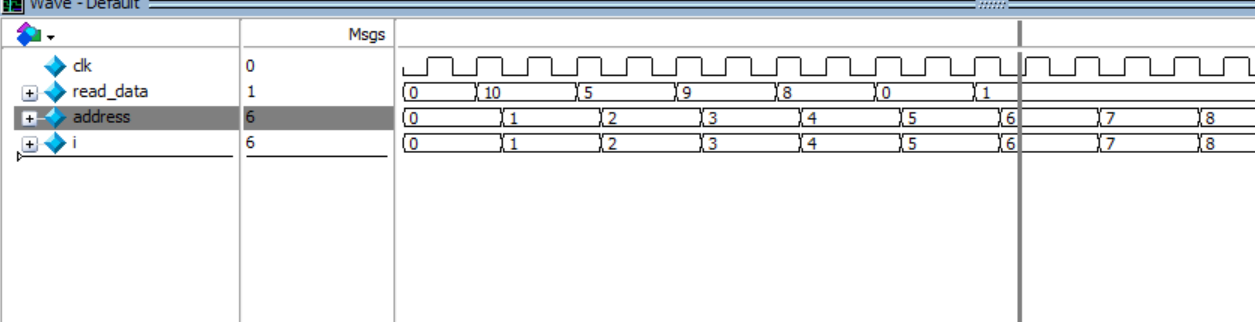
4、仿真结果
5、结果
ROM配置较为简单,但也是非常实用的,由于本人水平有限,只能作为自己一个复习的标准,可能描述的不是很详细,大家可以观看这个视频,描述的很详细
05_IP核之ROM使用讲解_哔哩哔哩_bilibili