日常·唠嗑
不知不觉,从开始接触Litedram已经过去了4个月,期间断断续续做了好多其他任务,导致进度比较慢,直到前天才把Litedram完全仿真起来。(坑很多,很多东西需要注意)
目录
- 日常·唠嗑
- 一、AXI用户接口bug
- 二、仿真程序
- 1、仿真结果
- 2、vivado工程目录:
- 3、example_top.v 例化转接桥:
一、AXI用户接口bug
Litedram官方给的AXI用户接口,在进行读写的时候,是有bug的,在写转NATIVE写的过程中,智能缓存16位数据,没有走DQ到DDR。(axi_0_wdata写数据,最后只写入storage_10,native接口可以正常读写)。
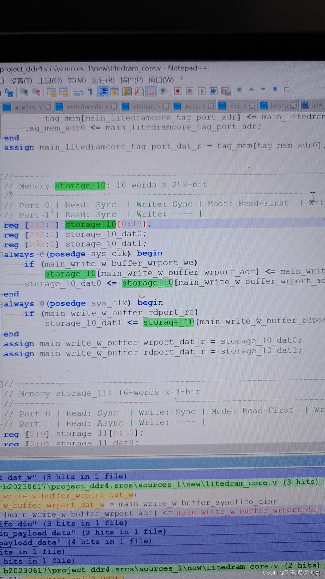
那么要解决这个问题,就只能产生wishbone用户接口或者native用户接口的litedram_core.v,然后再通过接口转换,替换成AXI协议的用户接口(转接桥设计)。另外需要注意的是,litedram的wishbone接口少了stall信号,需要将ack取反充当stall信号。
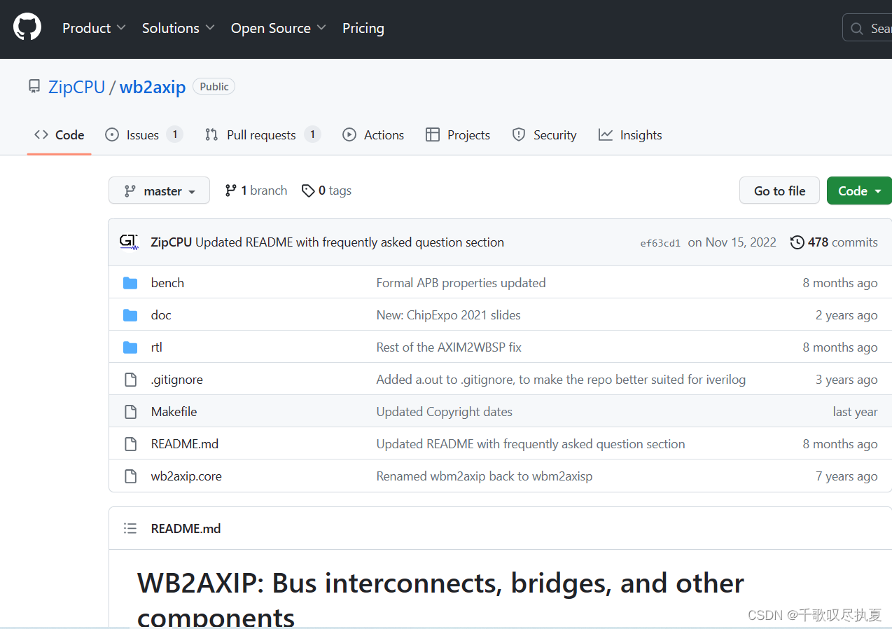
WB2AXIP转接桥:
https://github.com/ZipCPU/wb2axip
二、仿真程序
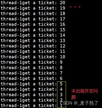
1、仿真结果
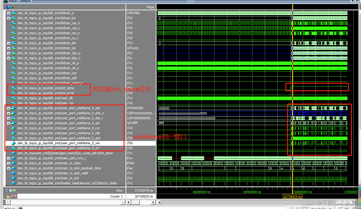
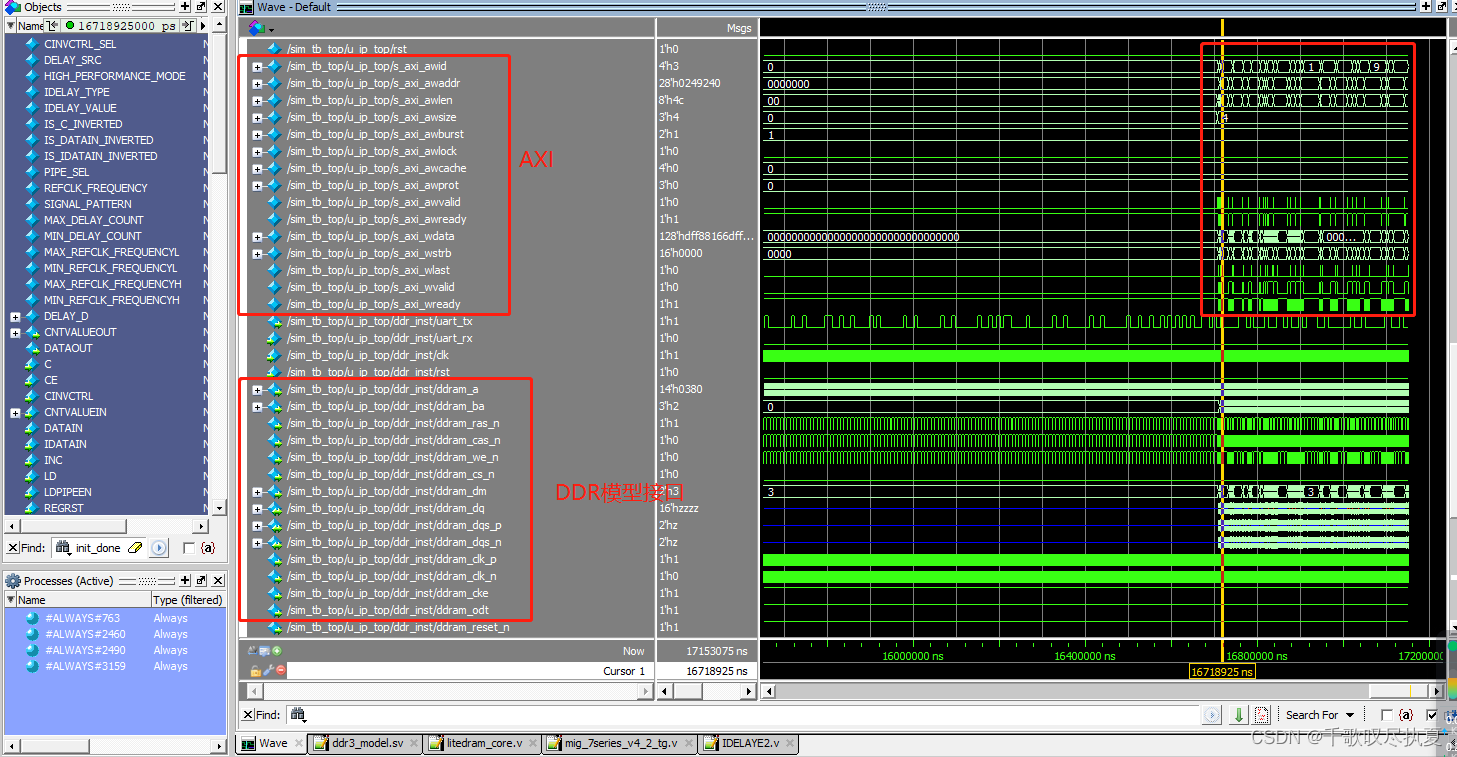
使用Xilinx 7系列FPGA的MIG AXI example例子进行仿真(将MIG控制器直接替换成litedram控制器)。
仿真结果:
从仿真结果可以看到,AXI数据跟Wishbone数据一直,并且读写到仿真模型里面。(仿真的时候,记得将litedram_core_rom.init&litedram_core_sram.init文件放到modelsim仿真工程下)
2、vivado工程目录:
我使用的是vivado2019.2跟modelsim 2019联合仿真的,具体步骤百度很多,自己检索。单独使用vivado自带的仿真器也是可以的。
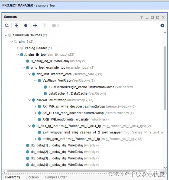
3、example_top.v 例化转接桥:
//*****************************************************************************
// (c) Copyright 2009 - 2013 Xilinx, Inc. All rights reserved.
//
// This file contains confidential and proprietary information
// of Xilinx, Inc. and is protected under U.S. and
// international copyright and other intellectual property
// laws.
//
// DISCLAIMER
// This disclaimer is not a license and does not grant any
// rights to the materials distributed herewith. Except as
// otherwise provided in a valid license issued to you by
// Xilinx, and to the maximum extent permitted by applicable
// law: (1) THESE MATERIALS ARE MADE AVAILABLE "AS IS" AND
// WITH ALL FAULTS, AND XILINX HEREBY DISCLAIMS ALL WARRANTIES
// AND CONDITIONS, EXPRESS, IMPLIED, OR STATUTORY, INCLUDING
// BUT NOT LIMITED TO WARRANTIES OF MERCHANTABILITY, NON-
// INFRINGEMENT, OR FITNESS FOR ANY PARTICULAR PURPOSE; and
// (2) Xilinx shall not be liable (whether in contract or tort,
// including negligence, or under any other theory of
// liability) for any loss or damage of any kind or nature
// related to, arising under or in connection with these
// materials, including for any direct, or any indirect,
// special, incidental, or consequential loss or damage
// (including loss of data, profits, goodwill, or any type of
// loss or damage suffered as a result of any action brought
// by a third party) even if such damage or loss was
// reasonably foreseeable or Xilinx had been advised of the
// possibility of the same.
//
// CRITICAL APPLICATIONS
// Xilinx products are not designed or intended to be fail-
// safe, or for use in any application requiring fail-safe
// performance, such as life-support or safety devices or
// systems, Class III medical devices, nuclear facilities,
// applications related to the deployment of airbags, or any
// other applications that could lead to death, personal
// injury, or severe property or environmental damage
// (individually and collectively, "Critical
// Applications"). Customer assumes the sole risk and
// liability of any use of Xilinx products in Critical
// Applications, subject only to applicable laws and
// regulations governing limitations on product liability.
//
// THIS COPYRIGHT NOTICE AND DISCLAIMER MUST BE RETAINED AS
// PART OF THIS FILE AT ALL TIMES.
//
//*****************************************************************************
// ____ ____
// / /\/ /
// /___/ \ / Vendor : Xilinx
// \ \ \/ Version : 4.2
// \ \ Application : MIG
// / / Filename : example_top.v
// /___/ /\ Date Last Modified : $Date: 2011/06/02 08:35:03 $
// \ \ / \ Date Created : Tue Sept 21 2010
// \___\/\___\
//
// Device : 7 Series
// Design Name : DDR3 SDRAM
// Purpose :
// Top-level module. This module serves as an example,
// and allows the user to synthesize a self-contained design,
// which they can be used to test their hardware.
// In addition to the memory controller, the module instantiates:
// 1. Synthesizable testbench - used to model user's backend logic
// and generate different traffic patterns
// Reference :
// Revision History :
//*****************************************************************************
//`define SKIP_CALIB
`timescale 1ps/1ps
`default_nettype wire
module example_top #
(
//***************************************************************************
// Traffic Gen related parameters
//***************************************************************************
parameter BEGIN_ADDRESS = 32'h00000000,
parameter END_ADDRESS = 32'h00ffffff,
parameter PRBS_EADDR_MASK_POS = 32'hff000000,
parameter ENFORCE_RD_WR = 0,
parameter ENFORCE_RD_WR_CMD = 8'h11,
parameter ENFORCE_RD_WR_PATTERN = 3'b000,
parameter C_EN_WRAP_TRANS = 0,
parameter C_AXI_NBURST_TEST = 0,
//***************************************************************************
// The following parameters refer to width of various ports
//***************************************************************************
parameter CK_WIDTH = 1,
// # of CK/CK# outputs to memory.
parameter nCS_PER_RANK = 1,
// # of unique CS outputs per rank for phy
parameter CKE_WIDTH = 1,
// # of CKE outputs to memory.
parameter DM_WIDTH = 2,
// # of DM (data mask)
parameter ODT_WIDTH = 1,
// # of ODT outputs to memory.
parameter BANK_WIDTH = 3,
// # of memory Bank Address bits.
parameter COL_WIDTH = 10,
// # of memory Column Address bits.
parameter CS_WIDTH = 1,
// # of unique CS outputs to memory.
parameter DQ_WIDTH = 16,
// # of DQ (data)
parameter DQS_WIDTH = 2,
parameter DQS_CNT_WIDTH = 1,
// = ceil(log2(DQS_WIDTH))
parameter DRAM_WIDTH = 8,
// # of DQ per DQS
parameter ECC = "OFF",
parameter ECC_TEST = "OFF",
//parameter nBANK_MACHS = 4,
parameter nBANK_MACHS = 8,
parameter RANKS = 1,
// # of Ranks.
parameter ROW_WIDTH = 14,
// # of memory Row Address bits.
parameter ADDR_WIDTH = 28,
// # = RANK_WIDTH + BANK_WIDTH
// + ROW_WIDTH + COL_WIDTH;
// Chip Select is always tied to low for
// single rank devices
//***************************************************************************
// The following parameters are mode register settings
//***************************************************************************
parameter BURST_MODE = "8",
// DDR3 SDRAM:
// Burst Length (Mode Register 0).
// # = "8", "4", "OTF".
// DDR2 SDRAM:
// Burst Length (Mode Register).
// # = "8", "4".
//***************************************************************************
// The following parameters are multiplier and divisor factors for PLLE2.
// Based on the selected design frequency these parameters vary.
//***************************************************************************
parameter CLKIN_PERIOD = 5000,
// Input Clock Period
parameter CLKFBOUT_MULT = 4,
// write PLL VCO multiplier
parameter DIVCLK_DIVIDE = 1,
// write PLL VCO divisor
parameter CLKOUT0_PHASE = 0.0,
// Phase for PLL output clock (CLKOUT0)
parameter CLKOUT0_DIVIDE = 1,
// VCO output divisor for PLL output clock (CLKOUT0)
parameter CLKOUT1_DIVIDE = 2,
// VCO output divisor for PLL output clock (CLKOUT1)
parameter CLKOUT2_DIVIDE = 32,
// VCO output divisor for PLL output clock (CLKOUT2)
parameter CLKOUT3_DIVIDE = 8,
// VCO output divisor for PLL output clock (CLKOUT3)
parameter MMCM_VCO = 800,
// Max Freq (MHz) of MMCM VCO
parameter MMCM_MULT_F = 8,
// write MMCM VCO multiplier
parameter MMCM_DIVCLK_DIVIDE = 1,
// write MMCM VCO divisor
//***************************************************************************
// Simulation parameters
//***************************************************************************
parameter SIMULATION = "FALSE",
// Should be TRUE during design simulations and
// FALSE during implementations
//***************************************************************************
// IODELAY and PHY related parameters
//***************************************************************************
parameter TCQ = 100,
parameter DRAM_TYPE = "DDR3",
//***************************************************************************
// System clock frequency parameters
//***************************************************************************
parameter nCK_PER_CLK = 4,
// # of memory CKs per fabric CLK
//***************************************************************************
// AXI4 Shim parameters
//***************************************************************************
parameter C_S_AXI_ID_WIDTH = 4,
// Width of all master and slave ID signals.
// # = >= 1.
parameter C_S_AXI_ADDR_WIDTH = 28,
// Width of S_AXI_AWADDR, S_AXI_ARADDR, M_AXI_AWADDR and
// M_AXI_ARADDR for all SI/MI slots.
// # = 32.
parameter C_S_AXI_DATA_WIDTH = 128,
// Width of WDATA and RDATA on SI slot.
// Must be <= APP_DATA_WIDTH.
// # = 32, 64, 128, 256.
parameter C_S_AXI_SUPPORTS_NARROW_BURST = 0,
// Indicates whether to instatiate upsizer
// Range: 0, 1
//***************************************************************************
// Debug parameters
//***************************************************************************
parameter DEBUG_PORT = "OFF",
// # = "ON" Enable debug signals/controls.
// = "OFF" Disable debug signals/controls.
parameter RST_ACT_LOW = 1
// =1 for active low reset,
// =0 for active high.
)
(
// Inouts
inout [15:0] ddr3_dq,
inout [1:0] ddr3_dqs_n,
inout [1:0] ddr3_dqs_p,
// Outputs
output [13:0] ddr3_addr,
output [2:0] ddr3_ba,
output ddr3_ras_n,
output ddr3_cas_n,
output ddr3_we_n,
output ddr3_reset_n,
output [0:0] ddr3_ck_p,
output [0:0] ddr3_ck_n,
output [0:0] ddr3_cke,
output [0:0] ddr3_cs_n,
output [1:0] ddr3_dm,
output [0:0] ddr3_odt,
// Inputs
// Single-ended system clock
input sys_clk_i,
output tg_compare_error,
output init_calib_complete,
// System reset - Default polarity of sys_rst pin is Active Low.
// System reset polarity will change based on the option
// selected in GUI.
input sys_rst
);
function integer clogb2 (input integer size);
begin
size = size - 1;
for (clogb2=1; size>1; clogb2=clogb2+1)
size = size >> 1;
end
endfunction // clogb2
function integer STR_TO_INT;
input [7:0] in;
begin
if(in == "8")
STR_TO_INT = 8;
else if(in == "4")
STR_TO_INT = 4;
else
STR_TO_INT = 0;
end
endfunction
localparam DATA_WIDTH = 16;
localparam RANK_WIDTH = clogb2(RANKS);
localparam PAYLOAD_WIDTH = (ECC_TEST == "OFF") ? DATA_WIDTH : DQ_WIDTH;
localparam BURST_LENGTH = STR_TO_INT(BURST_MODE);
localparam APP_DATA_WIDTH = 2 * nCK_PER_CLK * PAYLOAD_WIDTH;
localparam APP_MASK_WIDTH = APP_DATA_WIDTH / 8;
//***************************************************************************
// Traffic Gen related parameters (derived)
//***************************************************************************
localparam TG_ADDR_WIDTH = ((CS_WIDTH == 1) ? 0 : RANK_WIDTH)
+ BANK_WIDTH + ROW_WIDTH + COL_WIDTH;
localparam MASK_SIZE = DATA_WIDTH/8;
localparam DBG_WR_STS_WIDTH = 40;
localparam DBG_RD_STS_WIDTH = 40;
// Wire declarations
wire clk;
wire rst;
wire mmcm_locked;
reg aresetn;
wire app_sr_active;
wire app_ref_ack;
wire app_zq_ack;
wire app_rd_data_valid;
wire [APP_DATA_WIDTH-1:0] app_rd_data;
wire mem_pattern_init_done;
wire cmd_err;
wire data_msmatch_err;
wire write_err;
wire read_err;
wire test_cmptd;
wire write_cmptd;
wire read_cmptd;
wire cmptd_one_wr_rd;
// Slave Interface Write Address Ports
wire [C_S_AXI_ID_WIDTH-1:0] s_axi_awid;
wire [C_S_AXI_ADDR_WIDTH-1:0] s_axi_awaddr;
wire [7:0] s_axi_awlen;
wire [2:0] s_axi_awsize;
wire [1:0] s_axi_awburst;
wire [0:0] s_axi_awlock;
wire [3:0] s_axi_awcache;
wire [2:0] s_axi_awprot;
wire s_axi_awvalid;
wire s_axi_awready;
// Slave Interface Write Data Ports
wire [C_S_AXI_DATA_WIDTH-1:0] s_axi_wdata;
wire [(C_S_AXI_DATA_WIDTH/8)-1:0] s_axi_wstrb;
wire s_axi_wlast;
wire s_axi_wvalid;
wire s_axi_wready;
// Slave Interface Write Response Ports
wire s_axi_bready;
wire [C_S_AXI_ID_WIDTH-1:0] s_axi_bid;
wire [1:0] s_axi_bresp;
wire s_axi_bvalid;
// Slave Interface Read Address Ports
wire [C_S_AXI_ID_WIDTH-1:0] s_axi_arid;
wire [C_S_AXI_ADDR_WIDTH-1:0] s_axi_araddr;
wire [7:0] s_axi_arlen;
wire [2:0] s_axi_arsize;
wire [1:0] s_axi_arburst;
wire [0:0] s_axi_arlock;
wire [3:0] s_axi_arcache;
wire [2:0] s_axi_arprot;
wire s_axi_arvalid;
wire s_axi_arready;
// Slave Interface Read Data Ports
wire s_axi_rready;
wire [C_S_AXI_ID_WIDTH-1:0] s_axi_rid;
wire [C_S_AXI_DATA_WIDTH-1:0] s_axi_rdata;
wire [1:0] s_axi_rresp;
wire s_axi_rlast;
wire s_axi_rvalid;
wire cmp_data_valid;
wire [C_S_AXI_DATA_WIDTH-1:0] cmp_data; // Compare data
wire [C_S_AXI_DATA_WIDTH-1:0] rdata_cmp; // Read data
wire dbg_wr_sts_vld;
wire [DBG_WR_STS_WIDTH-1:0] dbg_wr_sts;
wire dbg_rd_sts_vld;
wire [DBG_RD_STS_WIDTH-1:0] dbg_rd_sts;
wire [11:0] device_temp;
`ifdef SKIP_CALIB
// skip calibration wires
wire calib_tap_req;
reg calib_tap_load;
reg [6:0] calib_tap_addr;
reg [7:0] calib_tap_val;
reg calib_tap_load_done;
`endif
//***************************************************************************
assign tg_compare_error = cmd_err | data_msmatch_err | write_err | read_err;
//assign tg_compare_error = cmd_err;
// Start of User Design top instance
//***************************************************************************
// The User design is instantiated below. The memory interface ports are
// connected to the top-level and the application interface ports are
// connected to the traffic generator module. This provides a reference
// for connecting the memory controller to system.
//***************************************************************************
wire init_done_out;
wire init_error_out;
assign init_calib_complete = ~init_error_out & init_done_out ;
//***************************************************************************
// The traffic generation module instantiated below drives traffic (patterns)
// on the application interface of the memory controller
//***************************************************************************
wire [23:0] axi2wb_adr ;
wire [127:0] axi2wb_dat_w ;
wire [127:0] axi2wb_dat_r ;
wire [15:0] axi2wb_sel ;
wire axi2wb_cyc ;
wire axi2wb_stb ;
wire axi2wb_ack ;
wire axi2wb_we ;
wire axi2wb_err ;
wire uart_tx;
wire uart_rx;
wire s_axi_wid;
assign uart_rx= 1'b0;
litedram_core ddr_inst(
.uart_tx (uart_tx),
.uart_rx (uart_rx),
.clk (sys_clk_i),
.rst (~sys_rst),
.pll_locked (),
.ddram_a (ddr3_addr),
.ddram_ba (ddr3_ba),
.ddram_ras_n (ddr3_ras_n),
.ddram_cas_n (ddr3_cas_n),
.ddram_we_n (ddr3_we_n),
.ddram_cs_n (ddr3_cs_n),
.ddram_dm (ddr3_dm),
.ddram_dq (ddr3_dq),
.ddram_dqs_p (ddr3_dqs_p),
.ddram_dqs_n (ddr3_dqs_n),
.ddram_clk_p (ddr3_ck_p),
.ddram_clk_n (ddr3_ck_n),
.ddram_cke (ddr3_cke),
.ddram_odt (ddr3_odt),
.ddram_reset_n (ddr3_reset_n),
.init_done (init_done_out),
.init_error (init_error_out),
.user_clk (clk),
.user_rst (rst),
.user_port_wishbone_0_adr (axi2wb_adr ),
.user_port_wishbone_0_dat_w (axi2wb_dat_w),
.user_port_wishbone_0_dat_r (axi2wb_dat_r),
.user_port_wishbone_0_sel (axi2wb_sel ),
.user_port_wishbone_0_cyc (axi2wb_cyc ),
.user_port_wishbone_0_stb (axi2wb_stb ),
.user_port_wishbone_0_ack (axi2wb_ack ),
.user_port_wishbone_0_we (axi2wb_we ),
.user_port_wishbone_0_err (axi2wb_err )
);
axim2wbsp #(
.C_AXI_ID_WIDTH (4), // The AXI id width used for R&W // This is an int between 1-16
.C_AXI_DATA_WIDTH (128),// Width of the AXI R&W data
.C_AXI_ADDR_WIDTH (28), // AXI Address width
.LGFIFO (5),
.OPT_SWAP_ENDIANNESS (0),
.OPT_READONLY (0),
.OPT_WRITEONLY (1'b0)
) axi2wb(
.S_AXI_ACLK (clk), // System clock
.S_AXI_ARESETN (~rst),
// AXI write address channel signals
.S_AXI_AWVALID (s_axi_awvalid),
.S_AXI_AWREADY (s_axi_awready),
.S_AXI_AWID (s_axi_awid),
.S_AXI_AWADDR (s_axi_awaddr),
.S_AXI_AWLEN (s_axi_awlen),
.S_AXI_AWSIZE (s_axi_arsize),
.S_AXI_AWBURST (s_axi_awburst),
.S_AXI_AWLOCK (s_axi_awlock[0]),
.S_AXI_AWCACHE (s_axi_awcache),
.S_AXI_AWPROT (s_axi_awprot),
.S_AXI_AWQOS (4'b1111),
// AXI write data channel signals
.S_AXI_WVALID (s_axi_wvalid),
.S_AXI_WREADY (s_axi_wready),
.S_AXI_WDATA (s_axi_wstrb),
.S_AXI_WSTRB (s_axi_wstrb),
.S_AXI_WLAST (s_axi_wlast),
// AXI write response channel signals
.S_AXI_BVALID (s_axi_bvalid),
.S_AXI_BREADY (s_axi_bready),
.S_AXI_BID (s_axi_bid),
.S_AXI_BRESP (s_axi_bresp),
// AXI read address channel signals
.S_AXI_ARVALID (s_axi_arvalid),
.S_AXI_ARREADY (s_axi_arready),
.S_AXI_ARID (s_axi_arid),
.S_AXI_ARADDR (s_axi_araddr),
.S_AXI_ARLEN (s_axi_arlen),
.S_AXI_ARSIZE (s_axi_arsize),
.S_AXI_ARBURST (s_axi_arlock),
.S_AXI_ARLOCK (s_axi_arlock),
.S_AXI_ARCACHE (s_axi_arcache),
.S_AXI_ARPROT (s_axi_arprot),
.S_AXI_ARQOS (4'b1111),
// AXI read data channel signals
.S_AXI_RVALID (s_axi_rvalid), // Rd rslt valid
.S_AXI_RREADY (s_axi_rready), // Rd rslt ready
.S_AXI_RID (s_axi_rid), // Response ID
.S_AXI_RDATA (s_axi_rdata),// Read data
.S_AXI_RLAST (s_axi_rlast), // Read last
.S_AXI_RRESP (s_axi_rresp), // Read response
// We'll share the clock and the reset
.o_reset (),
.o_wb_cyc (axi2wb_cyc),
.o_wb_stb (axi2wb_stb),
.o_wb_we (axi2wb_we),
.o_wb_addr (axi2wb_adr),
.o_wb_data (axi2wb_dat_w),
.o_wb_sel (axi2wb_sel),
.i_wb_stall (~axi2wb_ack),
.i_wb_ack (axi2wb_ack),
.i_wb_data (axi2wb_dat_r),
.i_wb_err (axi2wb_err)
);
//
always @(posedge clk) begin
aresetn <= ~rst;
end
mig_7series_v4_2_axi4_tg #(
.C_AXI_ID_WIDTH (C_S_AXI_ID_WIDTH),
.C_AXI_ADDR_WIDTH (C_S_AXI_ADDR_WIDTH),
.C_AXI_DATA_WIDTH (C_S_AXI_DATA_WIDTH),
.C_AXI_NBURST_SUPPORT (C_AXI_NBURST_TEST),
.C_EN_WRAP_TRANS (C_EN_WRAP_TRANS),
.C_BEGIN_ADDRESS (BEGIN_ADDRESS),
.C_END_ADDRESS (END_ADDRESS),
.PRBS_EADDR_MASK_POS (PRBS_EADDR_MASK_POS),
.DBG_WR_STS_WIDTH (DBG_WR_STS_WIDTH),
.DBG_RD_STS_WIDTH (DBG_RD_STS_WIDTH),
.ENFORCE_RD_WR (ENFORCE_RD_WR),
.ENFORCE_RD_WR_CMD (ENFORCE_RD_WR_CMD),
.EN_UPSIZER (C_S_AXI_SUPPORTS_NARROW_BURST),
.ENFORCE_RD_WR_PATTERN (ENFORCE_RD_WR_PATTERN)
) u_axi4_tg_inst
(
.aclk (clk),
.aresetn (aresetn),
// Input control signals
.init_cmptd (init_calib_complete),
.init_test (1'b0),
.wdog_mask (~init_calib_complete),
.wrap_en (1'b0),
// AXI write address channel signals
.axi_wready (s_axi_awready),
.axi_wid (s_axi_awid),
.axi_waddr (s_axi_awaddr),
.axi_wlen (s_axi_awlen),
.axi_wsize (s_axi_awsize),
.axi_wburst (s_axi_awburst),
.axi_wlock (s_axi_awlock),
.axi_wcache (s_axi_awcache),
.axi_wprot (s_axi_awprot),
.axi_wvalid (s_axi_awvalid),
// AXI write data channel signals
.axi_wd_wready (s_axi_wready),
.axi_wd_wid (s_axi_wid),
.axi_wd_data (s_axi_wdata),
.axi_wd_strb (s_axi_wstrb),
.axi_wd_last (s_axi_wlast),
.axi_wd_valid (s_axi_wvalid),
// AXI write response channel signals
.axi_wd_bid (s_axi_bid),
.axi_wd_bresp (s_axi_bresp),
.axi_wd_bvalid (s_axi_bvalid),
.axi_wd_bready (s_axi_bready),
// AXI read address channel signals
.axi_rready (s_axi_arready),
.axi_rid (s_axi_arid),
.axi_raddr (s_axi_araddr),
.axi_rlen (s_axi_arlen),
.axi_rsize (s_axi_arsize),
.axi_rburst (s_axi_arburst),
.axi_rlock (s_axi_arlock),
.axi_rcache (s_axi_arcache),
.axi_rprot (s_axi_arprot),
.axi_rvalid (s_axi_arvalid),
// AXI read data channel signals
.axi_rd_bid (s_axi_rid),
.axi_rd_rresp (s_axi_rresp),
.axi_rd_rvalid (s_axi_rvalid),
.axi_rd_data (s_axi_rdata),
.axi_rd_last (s_axi_rlast),
.axi_rd_rready (s_axi_rready),
// Error status signals
.cmd_err (cmd_err),
.data_msmatch_err (data_msmatch_err),
.write_err (write_err),
.read_err (read_err),
.test_cmptd (test_cmptd),
.write_cmptd (write_cmptd),
.read_cmptd (read_cmptd),
.cmptd_one_wr_rd (cmptd_one_wr_rd),
// Debug status signals
.cmp_data_en (cmp_data_valid),
.cmp_data_o (cmp_data),
.rdata_cmp (rdata_cmp),
.dbg_wr_sts_vld (dbg_wr_sts_vld),
.dbg_wr_sts (dbg_wr_sts),
.dbg_rd_sts_vld (dbg_rd_sts_vld),
.dbg_rd_sts (dbg_rd_sts)
);
wire dbg_sel_pi_incdec ;
wire dbg_sel_po_incdec ;
wire dbg_pi_f_inc ;
wire dbg_pi_f_dec ;
wire dbg_po_f_inc ;
wire dbg_po_f_dec ;
wire dbg_po_f_stg23_sel ;
wire po_win_tg_rst ;
wire vio_tg_rst ;
//*****************************************************************
// Default values are assigned to the debug inputs
//*****************************************************************
assign dbg_sel_pi_incdec = 'b0;
assign dbg_sel_po_incdec = 'b0;
assign dbg_pi_f_inc = 'b0;
assign dbg_pi_f_dec = 'b0;
assign dbg_po_f_inc = 'b0;
assign dbg_po_f_dec = 'b0;
assign dbg_po_f_stg23_sel = 'b0;
assign po_win_tg_rst = 'b0;
assign vio_tg_rst = 'b0;
`ifdef SKIP_CALIB
//***************************************************************************
// Skip calib test logic
//***************************************************************************
reg[3*DQS_WIDTH-1:0] po_coarse_tap;
reg[6*DQS_WIDTH-1:0] po_stg3_taps;
reg[6*DQS_WIDTH-1:0] po_stg2_taps;
reg[6*DQS_WIDTH-1:0] pi_stg2_taps;
reg[5*DQS_WIDTH-1:0] idelay_taps;
reg[11:0] cal_device_temp;
always @(posedge clk) begin
// tap values from golden run (factory)
po_coarse_tap <= #TCQ 'h2;
po_stg3_taps <= #TCQ 'h0D;
po_stg2_taps <= #TCQ 'h1D;
pi_stg2_taps <= #TCQ 'h1E;
idelay_taps <= #TCQ 'h08;
cal_device_temp <= #TCQ 'h000;
end
always @(posedge clk) begin
if (rst)
calib_tap_load <= #TCQ 1'b0;
else if (calib_tap_req)
calib_tap_load <= #TCQ 1'b1;
end
always @(posedge clk) begin
if (rst) begin
calib_tap_addr <= #TCQ 'd0;
calib_tap_val <= #TCQ po_coarse_tap[3*calib_tap_addr[6:3]+:3]; //'d1;
calib_tap_load_done <= #TCQ 1'b0;
end else if (calib_tap_load) begin
case (calib_tap_addr[2:0])
3'b000: begin
calib_tap_addr[2:0] <= #TCQ 3'b001;
calib_tap_val <= #TCQ po_stg3_taps[6*calib_tap_addr[6:3]+:6]; //'d19;
end
3'b001: begin
calib_tap_addr[2:0] <= #TCQ 3'b010;
calib_tap_val <= #TCQ po_stg2_taps[6*calib_tap_addr[6:3]+:6]; //'d45;
end
3'b010: begin
calib_tap_addr[2:0] <= #TCQ 3'b011;
calib_tap_val <= #TCQ pi_stg2_taps[6*calib_tap_addr[6:3]+:6]; //'d20;
end
3'b011: begin
calib_tap_addr[2:0] <= #TCQ 3'b100;
calib_tap_val <= #TCQ idelay_taps[5*calib_tap_addr[6:3]+:5]; //'d1;
end
3'b100: begin
if (calib_tap_addr[6:3] < DQS_WIDTH-1) begin
calib_tap_addr[2:0] <= #TCQ 3'b000;
calib_tap_val <= #TCQ po_coarse_tap[3*(calib_tap_addr[6:3]+1)+:3]; //'d1;
calib_tap_addr[6:3] <= #TCQ calib_tap_addr[6:3] + 1;
end else begin
calib_tap_addr[2:0] <= #TCQ 3'b110;
calib_tap_val <= #TCQ cal_device_temp[7:0];
calib_tap_addr[6:3] <= #TCQ 4'b1111;
end
end
3'b110: begin
calib_tap_addr[2:0] <= #TCQ 3'b111;
calib_tap_val <= #TCQ {4'h0,cal_device_temp[11:8]};
calib_tap_addr[6:3] <= #TCQ 4'b1111;
end
3'b111: begin
calib_tap_load_done <= #TCQ 1'b1;
end
endcase
end
end
//****************skip calib test logic end**********************************
`endif
endmodule