1、Pin Assignment & Description
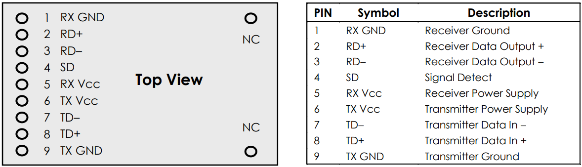
TD+, TD-:
DC coupled LVPECL inputs for the transmitter. 50Ω differential lines.
RD+, RD-:
Open-emitter out circuits. DC coupled LVPECL outputs for the receiver. 50Ω differential lines.
SD:
Signal Detect. Normal optical input levels to the receiver result in a logic “1” output, VOH, asserted. Low input optical levels to the receiver result in a fault condition indicated by a logic “0” output VOL, deasserted.
- SD is a single-ended LVPECL output and can be terminated with LVPECL techniques via 50 Ω to RX Vcc − 2V.
- Alternatively, SD can be loaded with a 180 Ω resistor to RX GND to conserve electrical power with small compromise to signal quality.
- If SD output is not used, leave it open-circuited. This SD output can be used to drive a LVPECL input on an upstream circuit, such as, SD input or Loss of Signal-bar. Connect to ground if not needed.
2、尺寸图

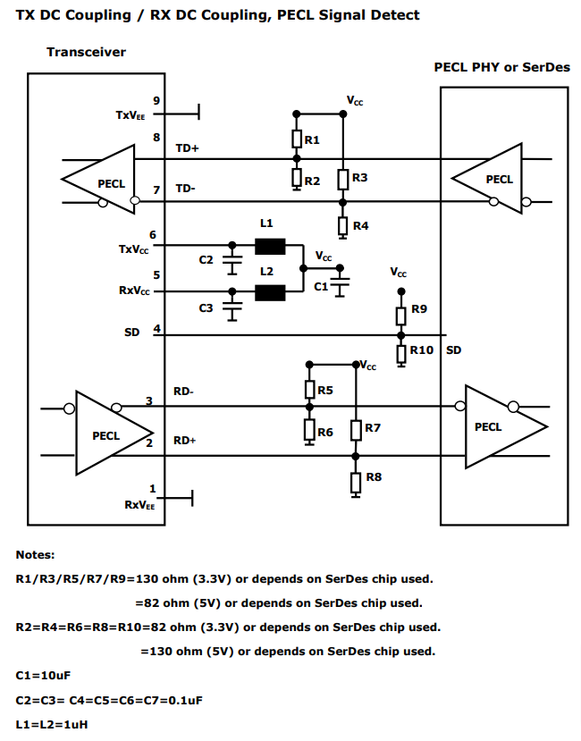
3、电路图
3.1、DC耦合:LVPECL互连
3.2、AC耦合

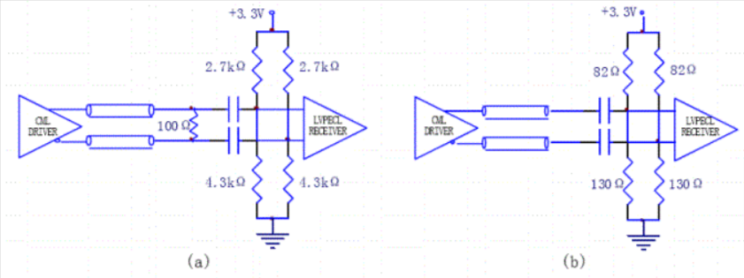
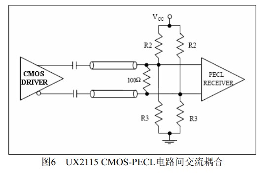
文献上的DC/AC Coupling描述可能都是错误的。
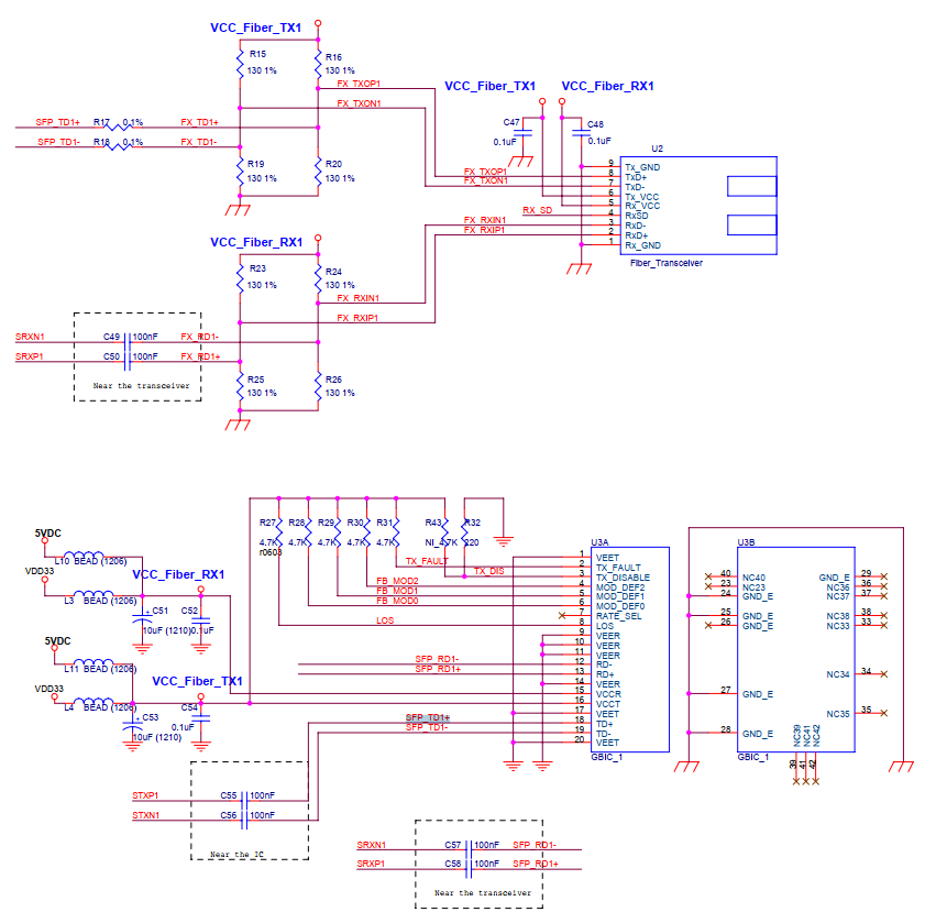
3.3、SFP和1X9 Co-lay原理图


![[附源码]计算机毕业设计大学生志愿者服务管理系统Springboot程序](https://img-blog.csdnimg.cn/40e3c265d5bf44af92f378b17e977ea8.png)

![[附源码]Python计算机毕业设计SSM基于微信平台的车险投保系统设计与实现(程序+LW)](https://img-blog.csdnimg.cn/9e1fcb8dd4df4505a4333c9a1d741b44.png)