FPGA 外置Flash的读写,用户数据存储
news2026/4/14 17:54:30
FPGA 外置Flash的读写用户数据存储前言一该功能验证平台及参考文章1Xilinx xc7k325tffg676-22vivado 2017.43验证的flash芯片MT25QL2564参考文章MT25QL256_datasheet5工程网盘链接https://pan.baidu.com/s/1HCBXLYvVRce5k5N_ro-3CA 提取码cyfo二、实现的功能1read Device ID2设置4-byte模式3flash的数据读写三部分代码总结前言大多数FPGA内部不具有掉电存储程序的功能所以都是外置flash存储器来存储程序上电后加载flash中的程序到FPGA中在运行。外置flash不仅可以作为存储程序使用也可以存储任何你想存储的用户数据这样可以更有效的利用flash的存储空间本文不讲其寄存器及原理这个网上很多。一该功能验证平台及参考文章1Xilinx xc7k325tffg676-22vivado 2017.43验证的flash芯片MT25QL2564参考文章MT25QL256_datasheet5工程网盘链接https://pan.baidu.com/s/1HCBXLYvVRce5k5N_ro-3CA 提取码cyfo二、实现的功能1read Device ID2设置4-byte模式3flash的数据读写三部分代码flash_spitimescale1ns/1ps//////////////////////////////////////////////////////////////////////////////////// Company:// Engineer: QSJ//// Create Date: 2021/03/26 9:02:44// Design Name:// Module Name: flash_spi// Project Name:// Target Devices:// Tool Versions:// Description://// Dependencies://// Revision:// Revision 0.01 - File Created// Additional Comments:////////////////////////////////////////////////////////////////////////////////////moduleflash_spi(input wire sys_clk,input wire i_rst_n,// ---------- spi port ---------output wire o_spi_clk,output wire o_spi_cs,output wire o_spi_mosi,input wire i_spi_miso,// --------- data port -----------input wire[7:0]iv_write_data,output reg o_wr_1_byte_ok,input wire[15:0]iv_write_num,input wire[15:0]iv_read_num,input wire[3:0]iv_cmd_type,output reg o_flash_done,input wire[7:0]iv_flash_cmd,input wire[31:0]iv_flash_addr,output reg[7:0]ov_read_data,output wire o_read_data_vld);wire spi_clk;reg spi_cs;reg spi_mosi;wire spi_miso;assign o_spi_clkspi_clk;assign o_spi_csspi_cs;assign o_spi_mosispi_mosi;assign spi_misoi_spi_miso;reg read_data_vld;reg[7:0]read_data;reg[2:0]spi_state;reg spi_clk_en1b0;reg data_come;assign o_read_data_vldread_data_vld;assign spi_clkspi_clk_en?sys_clk:0;parameter IDLE3b000;parameter CMD_SEND3b001;parameter ADDRESS_SEND3b010;parameter READ_WAIT3b011;parameter WRITE_DATA3b101;parameter FINISH_DONE3b110;reg[7:0]cmd_reg;reg[31:0]address_reg;reg[7:0]wr_bit_cnt;reg[15:0]write_cnt;reg[7:0]rd_bit_cnt;reg[15:0]read_cnt;reg[15:0]read_num_inner;reg read_finish;always (negedge sys_clk)beginif(!i_rst_n)begin spi_cs1b1;spi_stateIDLE;cmd_reg0;address_reg0;spi_clk_en1b0;wr_bit_cnt0;write_cnt0;read_num_inner0;o_flash_done1b0;data_come1b0;o_wr_1_byte_ok1b0;endelsebegincase(spi_state)IDLE:begin spi_clk_en1b0;spi_cs1b1;spi_mosi1b1;cmd_regiv_flash_cmd;address_regiv_flash_addr;o_flash_done1b0;if(iv_cmd_type[3]1b1)begin spi_stateCMD_SEND;wr_bit_cnt7;write_cnt0;read_num_inner0;end end CMD_SEND:begin spi_clk_en1b1;spi_cs1b0;if(wr_bit_cnt0)begin spi_mosicmd_reg[wr_bit_cnt];wr_bit_cntwr_bit_cnt-1b1;endelsebegin spi_mosicmd_reg[0];if((iv_cmd_type[2:0]3b001) | (iv_cmd_type[2:0]3b100))begin spi_stateFINISH_DONE;endelseif(iv_cmd_type[2:0]3b011)begin spi_stateREAD_WAIT;wr_bit_cnt7;read_num_inner1;endelseif(iv_cmd_type[2:0]3b000)begin spi_stateREAD_WAIT;wr_bit_cnt7;read_num_inner17;endelsebegin spi_stateADDRESS_SEND;wr_bit_cnt31;end end end ADDRESS_SEND:beginif(wr_bit_cnt0)begin spi_mosiaddress_reg[wr_bit_cnt];wr_bit_cntwr_bit_cnt-1;endelsebegin spi_mosiaddress_reg[0];if(iv_cmd_type[2:0]3b010)begin spi_stateFINISH_DONE;endelseif(iv_cmd_type[2:0]3b101)begin spi_stateWRITE_DATA;wr_bit_cnt7;endelsebegin spi_stateREAD_WAIT;read_num_inneriv_read_num;end end end READ_WAIT:beginif(read_finish)begin spi_stateFINISH_DONE;data_come1b0;endelsedata_come1b1;end WRITE_DATA:beginif(write_cntiv_write_num)beginif(wr_bit_cnt0)begin spi_mosiiv_write_data[wr_bit_cnt];wr_bit_cntwr_bit_cnt-1b1;o_wr_1_byte_ok1b0;endelsebegin spi_mosiiv_write_data[0];wr_bit_cnt7;o_wr_1_byte_ok1b1;write_cntwrite_cnt1b1;end endelsebegin spi_stateFINISH_DONE;spi_clk_en1b0;o_wr_1_byte_ok1b0;write_cnt0;end end FINISH_DONE:begin spi_cs1b1;spi_mosi1b1;spi_clk_en1b0;o_flash_done1b1;spi_stateIDLE;enddefault:spi_stateIDLE;endcase end end always (posedge sys_clk)beginif(!i_rst_n)begin read_cnt0;rd_bit_cnt0;read_finish1b0;read_data_vld1b0;read_data0;ov_read_data0;endelseif(data_come)beginif(read_cntread_num_inner)beginif(rd_bit_cnt7)begin read_data_vld1b0;read_data{read_data[6:0],spi_miso};rd_bit_cntrd_bit_cnt1b1;endelsebegin read_data_vld1b1;ov_read_data{read_data[6:0],spi_miso};rd_bit_cnt0;read_cntread_cnt1b1;end endelsebegin read_cnt0;read_finish1b1;read_data_vld1b0;end endelsebegin read_cnt0;rd_bit_cnt0;read_finish1b0;read_data_vld1b0;read_data0;end end endmoduleflash_cmdtimescale1ns/1ps//////////////////////////////////////////////////////////////////////////////////// Company:// Engineer: QSJ//// Create Date: 2021/03/26 9:04:02// Design Name:// Module Name: flash_cmd// Project Name:// Target Devices:// Tool Versions:// Description://// Dependencies://// Revision:// Revision 0.01 - File Created// Additional Comments:////////////////////////////////////////////////////////////////////////////////////moduleflash_cmd(input sys_clk,input i_rst_n,input i_wr_flash_start,input i_rd_flash_start,input i_rd_device_id_start,input i_subsector_erase_start,input wire[7:0]iv_write_data,output wire o_wr_1_byte_ok,input wire[15:0]iv_write_num,input wire[15:0]iv_read_num,input wire[31:0]iv_base_addr,output o_spi_clk,output o_spi_cs,output o_spi_mosi,input i_spi_miso,output[7:0]ov_rd_data,output o_rd_data_vld);reg[7:0]flash_cmd_def;reg[3:0]cmd_type;wire flash_done;wire[7:0]read_data;wire read_data_vld;reg[4:0]curr_stated15;always (posedge sys_clk)beginif(!i_rst_n)begin curr_stated15;flash_cmd_def8d0;cmd_type4b0000;endelsebegincase(curr_state)d0://idleif(i_wr_flash_start)curr_stated8;elseif(i_rd_flash_start)curr_stated13;elseif(i_rd_device_id_start)curr_stated1;elseif(i_subsector_erase_start)curr_stated3;elsecurr_stated0;// -------------- read device ID ------------------d1://Read Status Register:05Hif(flash_done)beginif(read_data[0]1b0)begin flash_cmd_def8h00;curr_stated2;cmd_type4b0000;endelsebegin flash_cmd_def8h05;cmd_type4b1011;end endelsebegin flash_cmd_def8h05;cmd_type4b1011;end d2:// Read Device ID:9FHif(flash_done)begin flash_cmd_def8h00;if(read_data8hFF)// if the device id is errorcurr_stated1;elsecurr_stated0;cmd_type4b0000;endelsebegin flash_cmd_def8h9f;curr_statecurr_state;cmd_type4b1000;end// -------------- Erase ------------------d3://Read Status Register:05Hif(flash_done)beginif(read_data[0]1b0)begin flash_cmd_def8h00;curr_stated4;cmd_type4b0000;endelsebegin flash_cmd_def8h05;cmd_type4b1011;end endelsebegin flash_cmd_def8h05;cmd_type4b1011;end d4://Write Enable:06Hif(flash_done)begin flash_cmd_def8h00;curr_stated5;cmd_type4b0000;endelsebegin flash_cmd_def8h06;curr_statecurr_state;cmd_type4b1001;end d5://4-byte address mode Sector Erase:DCH Subsector Erase:21Hif(flash_done)begin flash_cmd_def8h00;curr_stated6;cmd_type4b0000;endelsebegin flash_cmd_def8h21;curr_statecurr_state;cmd_type4b1010;end d6://Read Status Register:05Hif(flash_done)beginif(read_data[0]1b0)begin flash_cmd_def8h00;curr_stated7;cmd_type4b0000;endelsebegin flash_cmd_def8h05;cmd_type4b1011;end endelsebegin flash_cmd_def8h05;cmd_type4b1011;end d7://Write disable: 04Hif(flash_done)begin flash_cmd_def8h00;curr_stated0;cmd_type4b0000;endelsebegin flash_cmd_def8h04;cmd_type4b1100;end// -------------- write Data ------------------d8://Read Status Register:05Hif(flash_done)beginif(read_data[0]1b0)begin flash_cmd_def8h00;curr_stated9;cmd_type4b0000;endelsebegin flash_cmd_def8h05;cmd_type4b1011;end endelsebegin flash_cmd_def8h05;cmd_type4b1011;end d9://Write Enable:06Hif(flash_done)begin flash_cmd_def8h00;curr_stated10;cmd_type4b0000;endelsebegin flash_cmd_def8h06;cmd_type4b1001;end d10://4-byte address page program: write data to flashif(flash_done)begin flash_cmd_def8h00;curr_stated11;cmd_type4b0000;endelsebegin flash_cmd_def8h12;cmd_type4b1101;end d11://Read Status Register:05Hif(flash_done)beginif(read_data[0]1b0)begin flash_cmd_def8h00;curr_stated12;cmd_type4b0000;endelsebegin flash_cmd_def8h05;cmd_type4b1011;end endelsebegin flash_cmd_def8h05;cmd_type4b1011;end d12://Write disable: 04Hif(flash_done)begin flash_cmd_def8h00;curr_stated0;cmd_type4b0000;endelsebegin flash_cmd_def8h04;cmd_type4b1100;end// -------------- read Data ------------------d13://Read Status Register:05Hif(flash_done)beginif(read_data[0]1b0)begin flash_cmd_def8h00;curr_stated14;cmd_type4b0000;endelsebegin flash_cmd_def8h05;cmd_type4b1011;end endelsebegin flash_cmd_def8h05;cmd_type4b1011;end d14://4-byte address read flash dataif(flash_done)begin flash_cmd_def8h00;curr_stated0;cmd_type4b0000;endelsebegin flash_cmd_def8h13;cmd_type4b1110;end// -------------- enter 4-byte mode ------------------d15://Read Status Register:05Hif(flash_done)beginif(read_data[0]1b0)begin flash_cmd_def8h00;curr_stated16;cmd_type4b0000;endelsebegin flash_cmd_def8h05;cmd_type4b1011;end endelsebegin flash_cmd_def8h05;cmd_type4b1011;end d16://Write Enable:06Hif(flash_done)begin flash_cmd_def8h00;curr_stated17;cmd_type4b0000;endelsebegin flash_cmd_def8h06;cmd_type4b1001;end d17://Enter 4-byte address mode:B7Hif(flash_done)begin flash_cmd_def8h00;curr_stated18;cmd_type4b0000;endelsebegin flash_cmd_def8hB7;cmd_type4b1001;end d18://Read Status Register:05Hif(flash_done)beginif(read_data[0]1b0)begin flash_cmd_def8h00;curr_stated19;cmd_type4b0000;endelsebegin flash_cmd_def8h05;cmd_type4b1011;end endelsebegin flash_cmd_def8h05;cmd_type4b1011;end d19://Write disable: 04Hif(flash_done)begin flash_cmd_def8h00;curr_stated1;cmd_type4b0000;endelsebegin flash_cmd_def8h04;cmd_type4b1100;end endcase end end reg[31:0]base_addr;always (posedge sys_clk)beginif(!i_rst_n)begin base_addrd0;endelsebeginif(curr_state0)beginif(i_wr_flash_start|i_rd_flash_start|i_subsector_erase_start)base_addriv_base_addr;elsebase_addrd0;endelsebase_addrbase_addr;end end flash_spiU_flash_spi(.sys_clk(sys_clk),.i_rst_n(i_rst_n),.o_spi_clk(o_spi_clk),.o_spi_cs(o_spi_cs),.o_spi_mosi(o_spi_mosi),.i_spi_miso(i_spi_miso),.iv_write_data(iv_write_data),.o_wr_1_byte_ok(o_wr_1_byte_ok),.iv_write_num(iv_write_num),.iv_read_num(iv_read_num),.iv_cmd_type(cmd_type),.o_flash_done(flash_done),.iv_flash_cmd(flash_cmd_def),.iv_flash_addr(base_addr),.ov_read_data(read_data),.o_read_data_vld(read_data_vld));assign ov_rd_dataread_data;assign o_rd_data_vld(curr_stated14)?read_data_vld:0;endmodule总结以上就是全部内容仅做个人记录若需要对flash进行更多操作可阅读flash对应的datasheet。有完整的VIVADO FPGA测试工程。工程未经过全面的调试有问题请指正
本文来自互联网用户投稿,该文观点仅代表作者本人,不代表本站立场。本站仅提供信息存储空间服务,不拥有所有权,不承担相关法律责任。如若转载,请注明出处:http://www.coloradmin.cn/o/2517203.html
如若内容造成侵权/违法违规/事实不符,请联系多彩编程网进行投诉反馈,一经查实,立即删除!相关文章
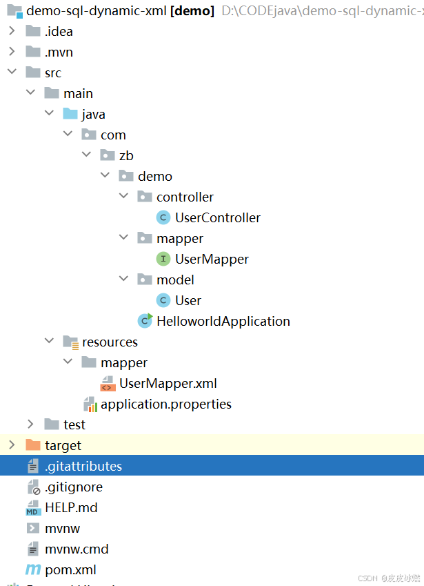
SpringBoot-17-MyBatis动态SQL标签之常用标签
文章目录 1 代码1.1 实体User.java1.2 接口UserMapper.java1.3 映射UserMapper.xml1.3.1 标签if1.3.2 标签if和where1.3.3 标签choose和when和otherwise1.4 UserController.java2 常用动态SQL标签2.1 标签set2.1.1 UserMapper.java2.1.2 UserMapper.xml2.1.3 UserController.ja…

wordpress后台更新后 前端没变化的解决方法
使用siteground主机的wordpress网站,会出现更新了网站内容和修改了php模板文件、js文件、css文件、图片文件后,网站没有变化的情况。
不熟悉siteground主机的新手,遇到这个问题,就很抓狂,明明是哪都没操作错误&#x…
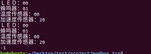
网络编程(Modbus进阶)
思维导图 Modbus RTU(先学一点理论)
概念 Modbus RTU 是工业自动化领域 最广泛应用的串行通信协议,由 Modicon 公司(现施耐德电气)于 1979 年推出。它以 高效率、强健性、易实现的特点成为工业控制系统的通信标准。 包…
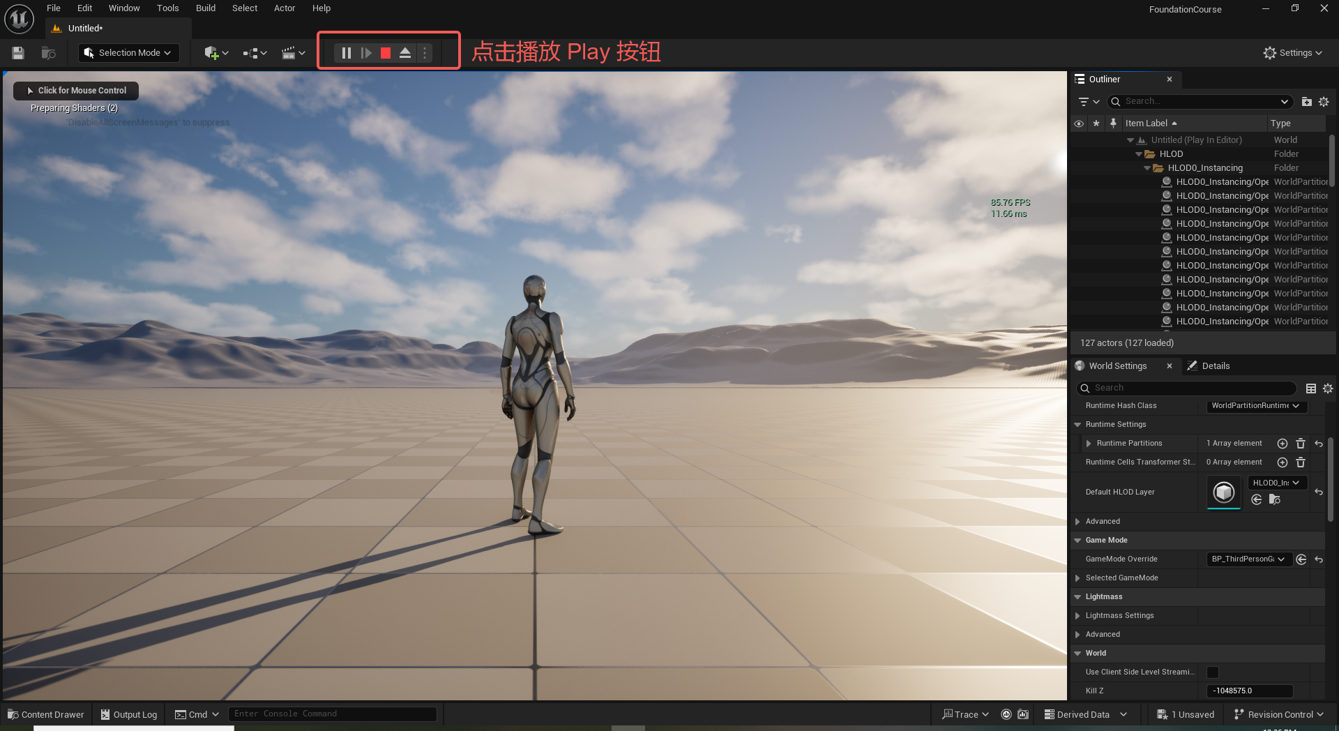
UE5 学习系列(二)用户操作界面及介绍
这篇博客是 UE5 学习系列博客的第二篇,在第一篇的基础上展开这篇内容。博客参考的 B 站视频资料和第一篇的链接如下:
【Note】:如果你已经完成安装等操作,可以只执行第一篇博客中 2. 新建一个空白游戏项目 章节操作,重…
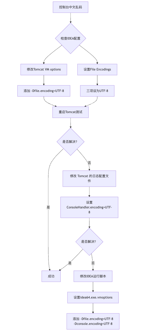
IDEA运行Tomcat出现乱码问题解决汇总
最近正值期末周,有很多同学在写期末Java web作业时,运行tomcat出现乱码问题,经过多次解决与研究,我做了如下整理:
原因:
IDEA本身编码与tomcat的编码与Windows编码不同导致,Windows 系统控制台…
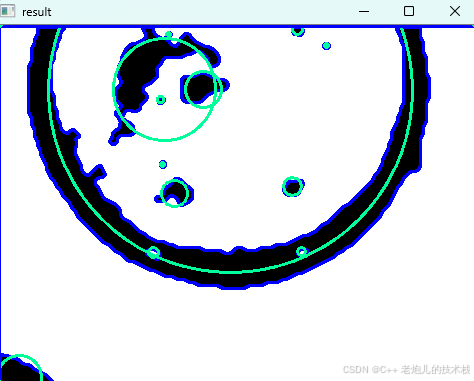
利用最小二乘法找圆心和半径
#include <iostream>
#include <vector>
#include <cmath>
#include <Eigen/Dense> // 需安装Eigen库用于矩阵运算 // 定义点结构
struct Point { double x, y; Point(double x_, double y_) : x(x_), y(y_) {}
}; // 最小二乘法求圆心和半径 …
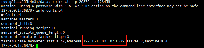
使用docker在3台服务器上搭建基于redis 6.x的一主两从三台均是哨兵模式
一、环境及版本说明
如果服务器已经安装了docker,则忽略此步骤,如果没有安装,则可以按照一下方式安装: 1. 在线安装(有互联网环境): 请看我这篇文章 传送阵>> 点我查看 2. 离线安装(内网环境):请看我这篇文章 传送阵>> 点我查看
说明:假设每台服务器已…
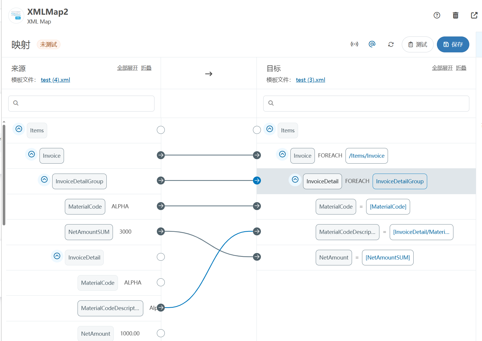
XML Group端口详解
在XML数据映射过程中,经常需要对数据进行分组聚合操作。例如,当处理包含多个物料明细的XML文件时,可能需要将相同物料号的明细归为一组,或对相同物料号的数量进行求和计算。传统实现方式通常需要编写脚本代码,增加了开…
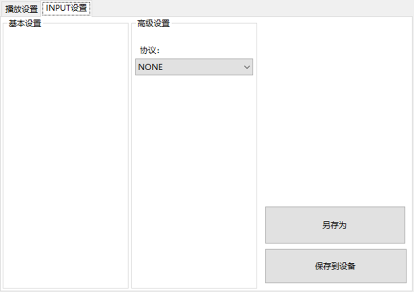
LBE-LEX系列工业语音播放器|预警播报器|喇叭蜂鸣器的上位机配置操作说明
LBE-LEX系列工业语音播放器|预警播报器|喇叭蜂鸣器专为工业环境精心打造,完美适配AGV和无人叉车。同时,集成以太网与语音合成技术,为各类高级系统(如MES、调度系统、库位管理、立库等)提供高效便捷的语音交互体验。
L…
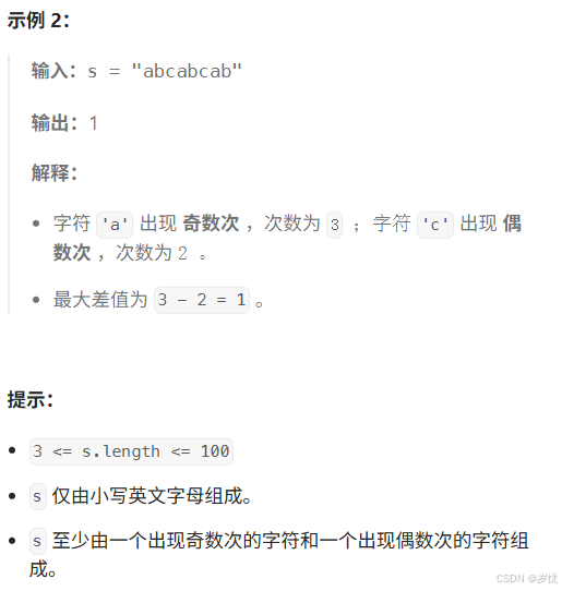
(LeetCode 每日一题) 3442. 奇偶频次间的最大差值 I (哈希、字符串)
题目:3442. 奇偶频次间的最大差值 I 思路 :哈希,时间复杂度0(n)。 用哈希表来记录每个字符串中字符的分布情况,哈希表这里用数组即可实现。
C版本:
class Solution {
public:int maxDifference(string s) {int a[26]…
【大模型RAG】拍照搜题技术架构速览:三层管道、两级检索、兜底大模型
摘要
拍照搜题系统采用“三层管道(多模态 OCR → 语义检索 → 答案渲染)、两级检索(倒排 BM25 向量 HNSW)并以大语言模型兜底”的整体框架: 多模态 OCR 层 将题目图片经过超分、去噪、倾斜校正后,分别用…

【Axure高保真原型】引导弹窗
今天和大家中分享引导弹窗的原型模板,载入页面后,会显示引导弹窗,适用于引导用户使用页面,点击完成后,会显示下一个引导弹窗,直至最后一个引导弹窗完成后进入首页。具体效果可以点击下方视频观看或打开下方…

接口测试中缓存处理策略
在接口测试中,缓存处理策略是一个关键环节,直接影响测试结果的准确性和可靠性。合理的缓存处理策略能够确保测试环境的一致性,避免因缓存数据导致的测试偏差。以下是接口测试中常见的缓存处理策略及其详细说明:
一、缓存处理的核…
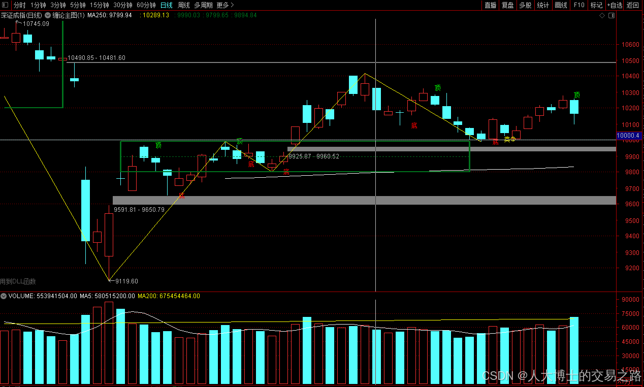
龙虎榜——20250610
上证指数放量收阴线,个股多数下跌,盘中受消息影响大幅波动。 深证指数放量收阴线形成顶分型,指数短线有调整的需求,大概需要一两天。 2025年6月10日龙虎榜行业方向分析 1. 金融科技
代表标的:御银股份、雄帝科技
驱动…
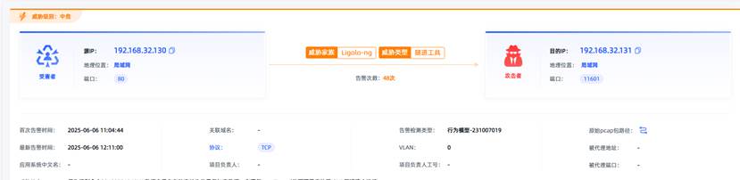
观成科技:隐蔽隧道工具Ligolo-ng加密流量分析
1.工具介绍
Ligolo-ng是一款由go编写的高效隧道工具,该工具基于TUN接口实现其功能,利用反向TCP/TLS连接建立一条隐蔽的通信信道,支持使用Let’s Encrypt自动生成证书。Ligolo-ng的通信隐蔽性体现在其支持多种连接方式,适应复杂网…
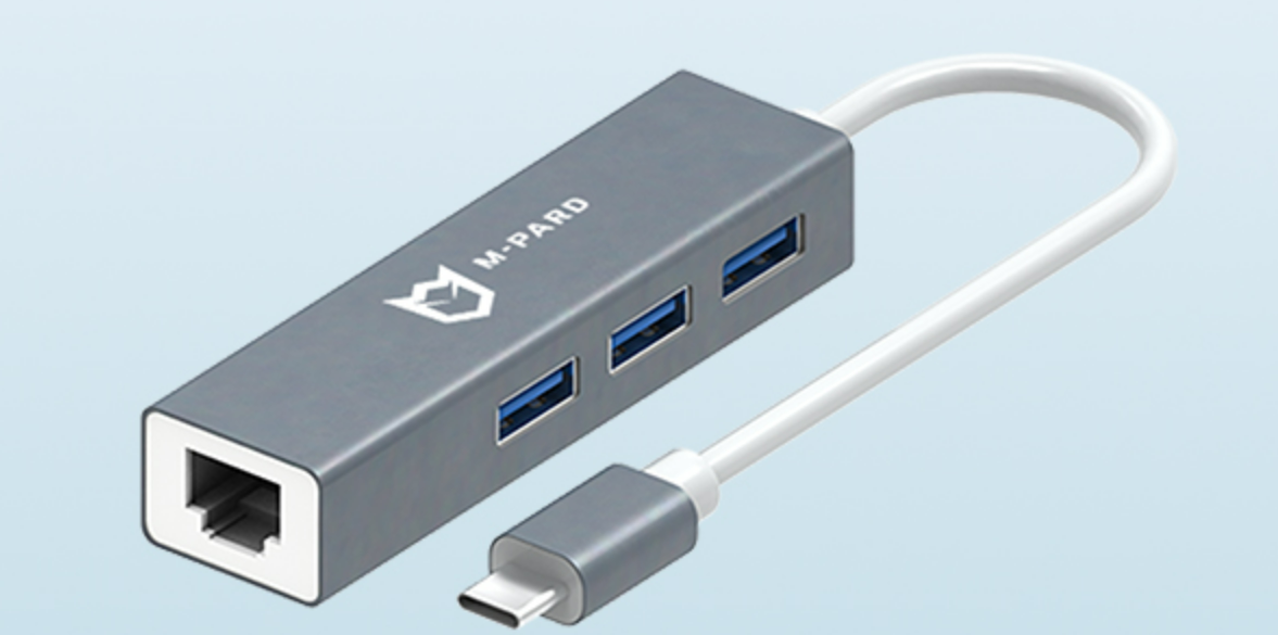
铭豹扩展坞 USB转网口 突然无法识别解决方法
当 USB 转网口扩展坞在一台笔记本上无法识别,但在其他电脑上正常工作时,问题通常出在笔记本自身或其与扩展坞的兼容性上。以下是系统化的定位思路和排查步骤,帮助你快速找到故障原因:
背景:
一个M-pard(铭豹)扩展坞的网卡突然无法识别了,扩展出来的三个USB接口正常。…
未来机器人的大脑:如何用神经网络模拟器实现更智能的决策?
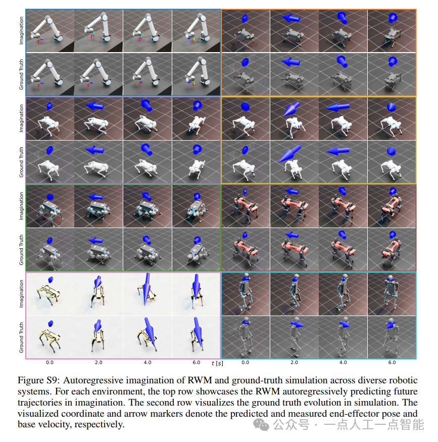
编辑:陈萍萍的公主一点人工一点智能 未来机器人的大脑:如何用神经网络模拟器实现更智能的决策?RWM通过双自回归机制有效解决了复合误差、部分可观测性和随机动力学等关键挑战,在不依赖领域特定归纳偏见的条件下实现了卓越的预测准…
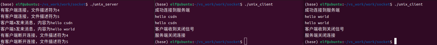
Linux应用开发之网络套接字编程(实例篇)
服务端与客户端单连接
服务端代码
#include <sys/socket.h>
#include <sys/types.h>
#include <netinet/in.h>
#include <stdio.h>
#include <stdlib.h>
#include <string.h>
#include <arpa/inet.h>
#include <pthread.h>
…

华为云AI开发平台ModelArts
华为云ModelArts:重塑AI开发流程的“智能引擎”与“创新加速器”!
在人工智能浪潮席卷全球的2025年,企业拥抱AI的意愿空前高涨,但技术门槛高、流程复杂、资源投入巨大的现实,却让许多创新构想止步于实验室。数据科学家…
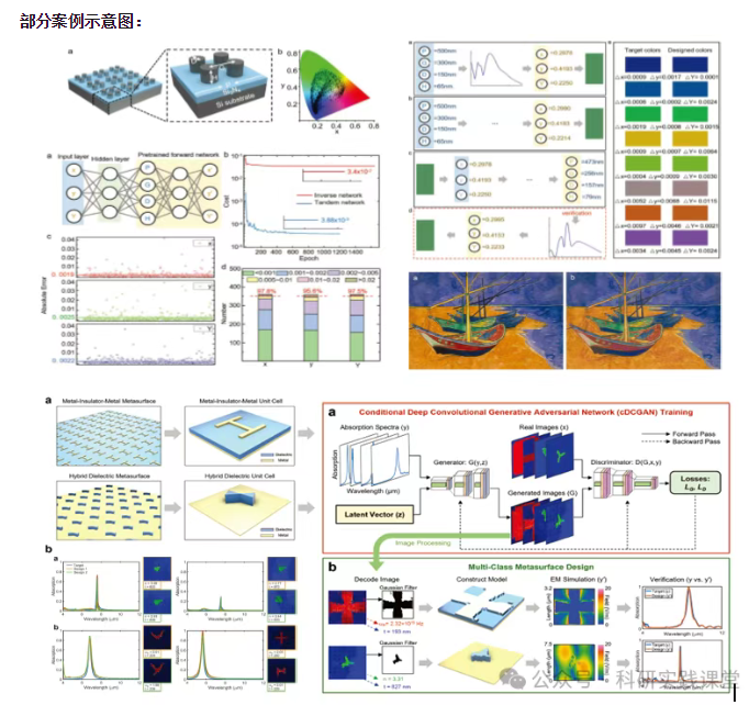
深度学习在微纳光子学中的应用
深度学习在微纳光子学中的主要应用方向
深度学习与微纳光子学的结合主要集中在以下几个方向:
逆向设计 通过神经网络快速预测微纳结构的光学响应,替代传统耗时的数值模拟方法。例如设计超表面、光子晶体等结构。
特征提取与优化 从复杂的光学数据中自…