视频链接
SDRAM电路设计01_哔哩哔哩_bilibili
SDRAM电路设计
1、SDRAM简介
SDRAM:Synchronous Dynamic Random Access Memory,同步动态随机存储器。
同步是指其时钟频率和CPU前端总线的系统时钟相同,并且内部命令的发送与数据的传输都以它为基准;
动态是指存储阵列需要不断的刷新来保证数据不丢失;
随机是指数据不是线性依次存储,而是自由指定地址进行数据的读写。
演变史:SDRAM从发展到现在已经经历了六代,分别是:第一代SDR SDRAM,第二代DDR SDRAM,第三代DDR2 SDRAM,第四代DDR3 SDRAM,第五代,DDR4 SDRAM。第六代,DDR5 SDRAM。
工作电压:SDR:3.3V DDR:2.5V DDR2:1.8V DDR3:1.5V DDR4:1.2V
2、SDRAM命名规范及尺寸
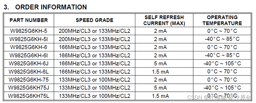
2.1、SDRAM命名规范
2.2、SDRAM封装(以华邦为例)
1、不同的厂家,封装有所出入。比如三星的SDRAM有SOP和BGA两种封装。
管脚定义(有些)相同,硬件设计时需要比较。
2、分X4、X8、X16三种类型。
3、SDRAM框图
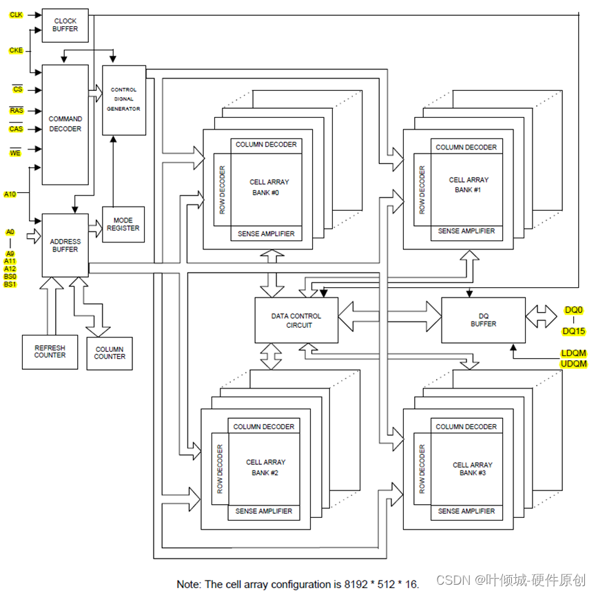
存储器主要包括指令译码器、地址线、数据线、存储块、模式寄存器和动态电路控制。
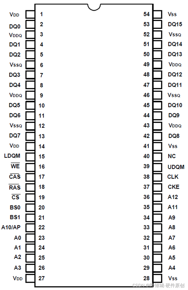
4、SDRAM管脚定义
SDRAM的管脚可以分为电源线、数据线、地址线和控制线。
4.1、电源线
对于电源电压,DDR SDRAM系统要求三个电源,分别为VDDQ、VTT和VREF。
| 管脚符号 | 类型 | 描述 |
| VDD | Supply | Power for input buffers and logic circuit inside DRAM. 用于DRAM内部输入缓冲器和逻辑电路的电源 |
| VSS | Supply | Ground:Ground for input buffers and logic circuit inside DRAM. 地。DRAM内部的输入缓冲器和逻辑电路的接地。 |
| VDDQ | Supply | Power for I/O Buffer:Separated power from VDD, to improve DQ noise immunity. I/O缓冲区的电源:将电源与VDD分离,提高DQ抗噪能力。 |
| VSSQ | Supply | Ground for I/O:Buffer Separated ground from VSS, to improve DQ noise immunity. I/O缓冲区的地,将地面与VSS分离,提高DQ抗噪能力。 |
4.2、数据、控制、地址
| 管脚符号 | 类型 | 描述 |
| CLK | Input | Clock Inputs:System clock used to sample inputs on the rising edge of clock. 时钟输入:系统时钟用于采样时钟上升沿上的输入。 |
| DQ0-DQ15 | I/O | Multiplexed pins for data output and input. 数据输出和输入的多路引脚。 |
| LDQM UDQM | Input | Input/Output Mask:The output buffer is placed at Hi-Z when DQM is sampled high in read cycle. In write cycle, sampling DQM high will block the write operation with zero latency. |
| CKE | Input | Clock Enable:CKE controls the clock activation and deactivation. When CKE is low, Power Down mode, Suspend mode, or Self Refresh mode is entered. |
| CS# | Input | Chip Select:Disable or enable the command decoder. When command decoder is disabled, new command is ignored and previous operation continues. |
| BS0 BS1 | Input | Bank Select:Select bank to activate during row address latch time, or bank to read/write during address latch time. |
| A0-A12 | Input | Address:A0-A8 Multiplexed pins for row and column address. Row address: A0-A12. Column address: A0-A8. A10 is sampled during a precharge command to determine if all banks are to be precharged or bank selected by BS0, BS1. |
| RAS#、CAS#、WE# | Input | Row Address Strobe、Column Address Strobe、Write Enable. RAS#:列地址选通;CAS#:行地址选通;WE#:写使能。 |
DAT[15:0] 16根
A[12:0] 13根
CLK: 1根
CKE: 1根
CS: 1根
LDQM、UDQM: 2根
BA0、BA1: 2根
RAS#、CAS#、WE# 3根
NC: 1根
VDD: 3根
VDDQ: 4根
VSS 3根
VSSQ 4根
合计:40+14=54